



Heavy copper printed circuit boards (PCBs) ranging from 2oz to 10oz and beyond have become essential in today's world of electronics demanding increasing power density and thermal reliability. These are applied in many electric vehicles, renewable energy (RE) and power electronics (PE) systems. These high-strength substrates can withstand high current loads, provide better mechanical properties in load-bearing applications and, due to the reduced resistive loss, can even replace complicated busbars.
The material characteristics which make heavy copper highly desirable for power distribution, however, pose significant technical challenges in the downstream Surface Mount Technology (SMT) and Through-Hole Technology (THT) assembly processes. To change from standard 1oz copper to 2oz+ heavy copper, one has to make a fundamental change in chemical, mechanical and thermal parameters without incurring costly defects.
Thermal Management & Reflow Profiles
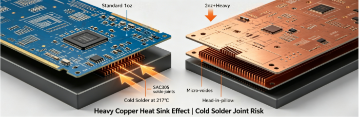
Massive Heat Sink Effect
Thermal properties are the major assembly challenge. The thickness of copper is the most important factor in significantly increasing the thermal capacity of the board. Thick copper traces and internal planes act as powerful heat sinks and rapidly remove heat from soldering pads during reflow soldering operations. The pad heating and the time necessary are not achievable through conventional reflow oven settings to achieve the 217°C liquidus temperature of the mainstream SAC305 lead-free solder.
Severe Cold Solder Joints
A lack of melting solder always results in cold joints, wetting problems and internal micro voids and head-in-pillow defects. These faults reduce the current carrying capacity and structural strength, and are a silent hazard of equipment failures during high current operation.
Profile Optimization Strategies
Engineers need to develop customized reflow thermal curves to tackle this issue. Longer soaking time is used to provide uniform thermal balance to thick copper parts; moderate heating rate is used to prevent damaging the heat-sensitive electronic parts. In the case of extra thick copper boards, auxiliary local infrared preheating or vapor phase soldering systems have been used to ensure uniform heating of the entire board.
Solder Mask Topography and Incomplete Coverage
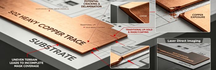
Heavy copper boards create uneven surface terrain, while standard PCs produce a smooth surface for easy application of solder mask. The copper traces on dielectric substrates are very prominent and have steep vertical side walls of 3oz or 5oz.
The traditional liquid photoimageable solder mask printing has difficulty in attaching evenly on the vertical edges. The coating ink will flow through sharp trace corners, exposing copper areas or even a thin coating. Screen printing also leaves air gaps next to thick traces and hides voids. In the follow up exposure and developing steps, the insufficient exposure of ultraviolet light will lead to mask undercut, which will cause cracking, peeling and delamination under high reflow temperature. The manufacturers use laser direct imaging and multi-layer printing with optimised printing inks to achieve stable and complete insulation coverage and avoid risks of electric arc.
Component Misalignment and Tombstoning
This is because the unbalanced copper layout caused by the wiring design and component placement results in severe warpage of the board. The expansion and contraction of thick copper structures are much more severe than those of FR-4 or polyimide base materials. In the pressing and reflow process, due to the mismatch of the thermal expansion coefficient, there is high internal stress, which affects the flatness of the board. The automatic placement machine does not achieve the stability of the placement of the parts, resulting in the misplacement of parts and circuit disconnections.
Thermal imbalance is another reason for tombstoning failure. If one component pad is connected to a thick copper power plane and the other pad is connected to a thin power line, the thin line is free to heat up and melt solder much faster than the thick copper side is heated. Surface tension of the solder is not even, causing components to be tilted and lifted. Such assembly failures can be effectively reduced by rational dummy copper layout and standard thermal relief design.
Stencil Design and Solder Paste Deposition
The solder paste surface is not regular and has mixed large and small components, which is difficult to achieve stable solder paste deposition. However, ordinary flat stencils can not be closely matched in the case of the stencil surface fluctuation, because there will be solder bridging and short circuit fault when printing with the paste.
Special stepped and 3D machined stencils are used to suit different surface elevations, for precise paste printing position and the same volume of coating. Electroless nickel immersion gold and immersion silver surface finishing treatments also improve the soldering quality of large size pads on heavy copper boards.
Automated SMT and Via Reliability Challenges
The heavier and thicker the heavy copper board is, the more difficult it will be to operate the automatic assembly equipment, and it will lead to the vibration of the conveyor, reduced vacuum absorption efficiency and inaccurate positioning recognition caused by local deformation of the board.
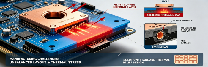
In the meantime thick copper layers put extreme thermal and mechanical pressure on plated through holes and vias. Hole wall cracks and damage to the resin due to shrinkage and layering after the repeated temperature changes result from the different speeds of expansion from the copper tube walls and the surrounding resin. High-Tg low-expansion base materials and low aspect ratio via design and filled thermal via arrays are used to maintain structural durability.
Through-Hole Solder Fillet Formation
Through-hole connectors and busbars are still used extensively in high-power electronic products to protect against vibration and high currents. Uneven heat dissipation makes it tough to meet standard vertical solder filling requirements. Heavy copper internal layers conduct heat fast during wave and selective soldering, causing liquid solder to harden half-way through holes. Unfilled joints will not produce good solder fillets. Increased heating time, increased solder temperature and increased preheating helps with filling effect, but has the trade-off of increased risk of board delamination and component overheating damage.
Achieving Assembly Excellence with PCBCart
The manufacture and assembly of 2oz+ heavy copper PCBs requires an assembly partner with material knowledge, state-of-the-art thermal profiling equipment and incredible inspection abilities.
PCBCart is a leading full turnkey PCB assembly and fabricationassembly service company with the engineering capability and up to date equipments to handle heavy copper projects. Whether it be Design for Manufacturability (DFM) analysis up front, for the best thermal reliefs, copper balancing or stencil adjustments, precision SMT assembly or automated optical inspection, or validation with X-ray analysis, PCBCart assures maximum production yields and proven reliability in the field. Partner with PCBCart to seamlessly transition your high-power electronics from conceptual design to flawless volume production.
Helpful Resources
• PCB Manufacturing Process A Step-by-Step Guide
• Printed Circuit Boards Assembly Process
• PCB Design File Requirements for Quick PCB Assembly Quote and Production
• How to Evaluate A PCB Manufacturer or A PCB Assembler
• Comparison between Wave Soldering and Reflow Soldering


