



The Dual Constraint: High Current and High-Voltage Isolation
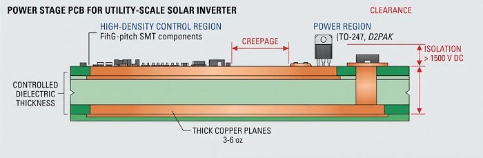
Power stage boards inside utility-scale solar inverters routinely carry per-string or per-module currents above 100 A, while the same board must maintain reliable isolation across DC bus voltages that increasingly sit above 1500 V in grid-scale string and central inverter architectures. These requirements pull board design in opposite directions: current capacity pushes toward thick copper (3–6 oz, occasionally heavier on bus-bar interconnect layers), while voltage isolation pushes toward tighter creepage/clearance management and controlled dielectric thickness.
Standard SMT parameters — stencil thickness, reflow profile, paste volume calculated for 1–2 oz copper — don't transfer directly to this stack-up. Heavy copper planes act as a large thermal mass during reflow, pulling heat from adjacent fine-pitch components and flattening the thermal gradient the profile was built for. Left unaddressed, this produces cold joints on large power pads alongside solder starvation or bridging on nearby fine-pitch parts. A power stage board is therefore two assembly problems coexisting on one panel: a fine-pitch driver/control region and a heavy-copper power region, each with different paste-volume and thermal requirements.
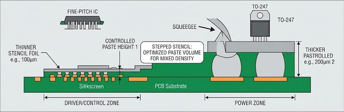
Stepped Stencil Design for Mixed-Density Power Boards
The practical response to this mismatch is a stepped, multi-thickness stencil rather than a single uniform foil. The driver/control zone — gate drivers, isolated gate driver ICs, current-sense amplifiers, fine-pitch passives — gets a thinner stencil section, where standard area-ratio rules apply to avoid insufficient paste release on small apertures. The power zone — discrete SiC/Si power device pads (TO-247, D2PAK/TO-263, power QFN/DFN), bus-bar landing pads, heavy-copper THT pad rings — gets a thicker, larger-aperture section, stepped up to deliver the paste volume large thermal-mass pads require without over-printing the smaller features nearby.
The aperture ratio difference between the two zones is the lever that matters: under-printing the power zone produces voiding and non-wetting on large pads even when the driver zone prints correctly, while over-printing it risks bridging nearby fine-pitch features. Because a stepped stencil creates two different target paste heights on one panel, print consistency has to be verified per zone rather than as a single panel average — paste deposits from both zones are measured with 3D Solder Paste Inspection (3D SPI) immediately after print, against zone-specific height and volume thresholds. 3D SPI here is a manufacturing-floor process-control check on print height and volume against a programmed target — a production capability, not an accredited metrology or calibration service — and its value is closed-loop: a paste-height deviation on either zone is caught and corrected before reflow, rather than surfacing later as a solder-joint defect on X-ray.
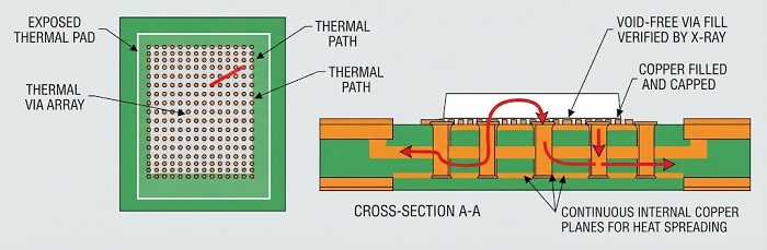
Thermal Via Arrays and Copper Fill for Power-Device Driver Boards
This section applies to discrete SiC/Si power devices reflow- or wave-soldered directly onto the board — TO-247, D2PAK/TO-263, and power QFN/DFN packages with an exposed thermal pad — not to bolt-down IGBT/SiC power modules with their own baseplate. Large modules mount to a heatsink mechanically, via screw or press-fit terminals, and their primary heat path runs through the module's own baseplate rather than the PCB; that mechanical attach sits outside standard PCBA assembly scope. For discrete devices, though, the thermal pad's only path to a heat spreader or copper pour is through the board, which makes the via strategy below core to assembly rather than an optional add-on.
The via array under a device's exposed thermal pad needs enough density that its combined cross-section approximates the pad footprint, rather than a sparse grid at the pad perimeter. Vias under these high-power footprints are typically copper-filled and capped rather than left open or resin-plugged, since an open via lets solder wick away from the joint during reflow and starves it. None of this works without plane continuity, though: internal copper planes tied to the thermal via field need enough continuous area to spread heat laterally, since a via array feeding a small, isolated copper island doesn't function as a heat sink no matter how well the vias are filled. Via fill quality and solder-joint integrity above the field are things the assembly process has to verify, not design-file assumptions to carry through untested.
Nitrogen Selective Wave Soldering for Heavy-Copper THT Terminals
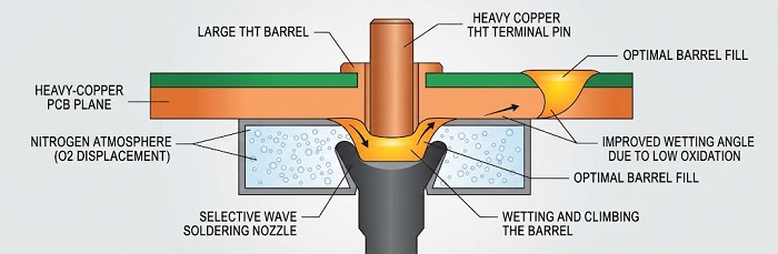
Utility-scale inverter power stages commonly retain through-hole components on the power path — busbar terminals, high-current inductors, connector blocks — where pad and barrel copper mass is large enough that hand soldering or standard reflow can't reliably achieve full barrel fill.
Copper oxidizes readily at elevated temperature in air, and an oxidized surface raises the contact angle between molten solder and base metal — in practical terms, the solder beads rather than wetting and climbing the barrel. On heavy-copper THT features this effect is magnified: the larger thermal mass keeps the joint at soldering temperature longer, giving oxidation more time to progress if the atmosphere isn't controlled. Nitrogen-protected selective wave soldering displaces ambient oxygen during solder-wave contact, improving wetting angle and barrel-fill consistency without the heavier flux loads that would otherwise compensate for poor wetting, and allowing a tighter, more repeatable dwell-time window since the process isn't fighting oxide formation in real time. On heavy-copper boards this runs as standard practice on ZSWHPS-11-2 equipment, not an optional upgrade — copper mass and terminal size here make oxidation-driven wetting failure a realistic outcome of an air-atmosphere wave process.
X-Ray Verification and Void Acceptance Criteria
Two defect modes are specific to this board type and aren't reliably caught by AOI alone, since both are subsurface: thermal-via fill voiding under discrete power device thermal pads, and solder-joint voiding beneath BGA/QFN control and driver ICs on the same board. Off-line X-ray, with oblique-angle capability, evaluates both — thermal via fill rate under the discrete device's thermal pad, since incomplete fill reduces the effective thermal path even when the surface solder joint looks acceptable, and BGA/QFN solder-joint voiding against IPC-7095D guidance. Worth being precise here: IPC-7095D is a process and inspection methodology document — how voids form, how to measure them by X-ray, how to structure a sampling plan — not the source of the numeric accept/reject line. The commonly cited void-area threshold (around 25% per solder ball under current guidance) comes from IPC-A-610, applied the same way across Class 2 and Class 3; what changes by class is inspection coverage, moving from lot sampling to 100% X-ray rather than a different percentage.
Because these boards mix a power-reliability-critical zone with a signal-integrity-critical zone, the practical acceptance approach isn't uniform across the panel: thermal vias under power devices are typically held to a stricter fill-rate criterion than general-purpose vias, while BGA/QFN packages get 100% X-ray coverage rather than sampling once the build calls for Class 3. X-ray data feeds back into the stencil and via-fill parameters above — a recurring void pattern in one zone signals a paste-volume or fill-sequence adjustment, not just a board to reject.
Why Prototype Iteration Matters on This Board Type
Heavy-copper power stage designs rarely arrive at final stencil zoning, via-fill parameters, and wave-solder settings on the first build — these are usually dialed in across two or three prototype runs, informed by SPI and X-ray data from the prior run, not derived correctly from the schematic and stack-up alone. That favors an assembly partner set up for high-mix, low-volume (HMLV) work: fast turnaround on a handful of boards, DFM feedback between iterations, and inspection data that feeds directly into the next batch's process parameters — rather than a line tuned once for a single validated design at volume. As an IATF 16949-certified HMLV assembler, this iteration cycle is closer to PCBCart's normal working mode than a one-shot high-volume run, and it matters more during a new design's validation phase than once the design is frozen.
DFM Self-Check List for Heavy-Copper Power Boards
● Power device package confirmed: discrete SMD/THT (solderable on this line) vs. bolt-down module with its own baseplate (mechanical attach, outside PCBA scope)
● Copper weight and current-carrying targets documented per net/plane
● Stencil zoned by aperture/thickness for driver vs. power regions, each with its own paste-height target
● Thermal via array sized to each discrete device's pad footprint, fill/cap method specified
● THT terminals and inductors on the power path flagged for nitrogen wave soldering, not reflow-only
● Panel warpage risk addressed at fixture level for large, asymmetric-copper layouts
● X-ray acceptance plan set separately for thermal-via fill under power devices vs. IPC-A-610/IPC-7095D-referenced BGA/QFN voiding, with inspection coverage (sampling vs. 100%) matched to build class
● Isolation/creepage clearances re-checked against the final copper layout, not just schematic intent
If you're scoping a solar or broader power-electronics project with a heavy-copper, high-current power stage, submit the board files and current/voltage requirements for a DFM and process-capability review.
Helpful Resources
● Relationship between Copper Weight, Trace Width and Current Carrying Capacity
● Selective Soldering ROI Reference: Manual vs. Automated THT Cost Comparison
● Managing Thermal Reliability in Diagnostic Instrument PCBA


