



A board that fails ICT isn't automatically a bad board. Two very different problems produce the same red “fail” on a test report: an actual manufacturing defect, and a test that couldn't make reliable contact in the first place. Confusing the two costs time in both directions — reworking a board that had a perfectly good joint but a bad contact wastes cycle time, and waving off every fail as “probably just the fixture” risks shipping a board with a real defect. This article covers the second category: false fails, sometimes called ghost failures, and the specific mechanisms behind them — flux residue, worn or under-pressured probes, and test point design.
What Counts as a False Fail in ICT?
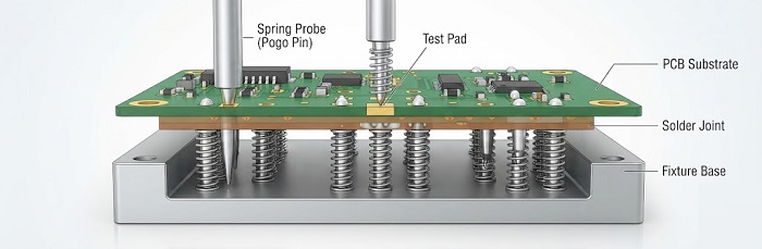
In-Circuit Testing makes contact with each test point through a bed of nails fixture — spring-loaded probes that land on designated pads to check for shorts, opens, and component values against expected parameters. A false fail happens when the fixture doesn't make a clean, low-resistance connection to a node that is, electrically, perfectly fine. The tester reports an open circuit or an out-of-tolerance reading not because the board is defective, but because the probe-to-pad contact itself is too resistive or intermittent.
Flux Residue and Probe Contact Resistance
No-clean flux is designed to stay on the board, and for the solder joint itself that's not a problem — a bulk joint doesn't need bare metal to conduct. A test point is a different story: the probe tip needs direct metal-to-metal contact with an exposed pad, and a film of flux residue sitting on that pad adds resistance right at the contact interface. Enough of it, and a probe reads an intermittent or high-resistance connection on a pad that would test fine if wiped clean first. This is the most common single root cause behind a false fail on boards that otherwise ran a clean, well-controlled process.

Probe Wear and Spring Pressure
Spring probes lose contact force gradually over their duty cycle — the spring weakens and the tip wears from repeated strikes, and contact resistance can drift upward well before a probe looks visibly worn. A fixture running probes near the end of their service life tends to produce false fails that cluster on the same handful of nodes across many boards, which is itself a useful diagnostic signal: a pattern repeating on the same node across a run points at the fixture, not the boards.
Test Point Design: Coverage, Size, and Tenting
Some false fails get designed in before the board is ever built. A test point sized smaller than the probe tip the fixture was built for, a via that's tented with solder mask when the test plan assumed exposed copper, or a node with no dedicated test point at all — relying instead on probing a component lead — all raise the odds of a poor or inconsistent contact regardless of how clean the process is. This is squarely a DFM issue, and it's a common finding in a design-for-test review ahead of first article rather than something process control alone can fix.
How Do You Tell a False Fail from a Real Defect?
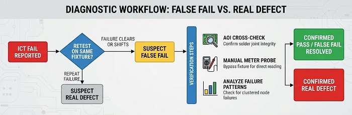
● Retest the same board on the same fixture. A genuine open or short repeats consistently; a contact-related false fail is more likely to shift or clear between retests
● Where possible, retest on a different fixture or probe set. A failure that follows the board is more likely real; one that disappears is more likely the fixture
● Cross-check with AOI or a manual meter probe placed directly on the pad, bypassing the ICT fixture entirely. A joint that reads fine by hand but fails on the bed of nails points to contact resistance, not a defect
● Look at the failure pattern across the lot. A real defect tends to be random or tied to a specific process excursion; a fixture problem tends to repeat on the same node across many boards
Why Does This Matter More for ATE and Semiconductor Test Boards?
False fails carry a specific cost on semiconductor ATE and test-interface boards. Every board pulled for a “failure” investigation is time off the line chasing a problem that may not exist, and finer pitch, higher test-point density on these boards leaves less margin for probe wear or flux residue before contact resistance becomes signal-relevant. There's a second, less visible risk too: a team that gets used to dismissing ICT fails as fixture noise can end up normalizing away a genuine defect on a board that's about to sit in a test cell — where a real open or short on the interface board gets misdiagnosed as a problem with the device under test instead, which is a considerably more expensive mistake to unwind than a rework on the flying probe test or ICT line itself.
Prevention and Process Controls
● Track probe contact resistance or strike count and replace on a defined schedule, rather than waiting for visible wear
● Control the no-clean flux process tightly, and where test point density is high, consider a cleaning step before ICT rather than relying on flux self-tolerance at the pad
● Run a design-for-test review during DFM: confirm test point size matches the fixture's probe tip spec, confirm no required test points are tented, and confirm every net that needs isolation has a dedicated accessible point
● Log false-fail patterns by node across lots through the fixture's traceability or MES system, so a node that fails repeatedly gets flagged as a likely fixture issue instead of being re-diagnosed as a new defect every time
● Keep a scheduled fixture preventive-maintenance plan rather than a purely reactive one
The practical takeaway: an ICT fail is the start of a diagnosis, not the end of one. Treating every fail as a confirmed defect leads to unnecessary rework and wasted cycle time; treating every fail as “probably the fixture” risks letting a real defect through. The distinction is almost always answerable with a retest, a cross-check against AOI, and a look at whether the failure clusters on a specific node.
Have an ICT fail pattern you're trying to diagnose? Get an Instant Quote for PCB Assembly
FAQs
1. What's the difference between a false fail and a real defect in ICT?
A false fail comes from the test fixture failing to make good contact with a good board — flux residue, worn probes, or a test point design issue. A real defect is an actual open, short, or out-of-spec component that would fail regardless of how the board was tested.
2. Can flux residue really cause a board to fail ICT if the solder joint itself is fine?
Yes — a probe needs direct metal-to-metal contact with an exposed test pad, and flux residue sitting on that pad adds resistance at the contact point even when the underlying solder joint is fully sound.
3. How often should ICT probes be replaced to avoid false fails?
Based on strike count or measured contact resistance drift, not visual wear — probes typically lose contact force well before they look worn.
4. Is a false fail a DFM issue or a process issue?
It can be either — undersized or tented test points are a DFM issue caught in design-for-test review, while flux residue and probe wear are process and fixture-maintenance issues.
5. Does AOI help distinguish a false fail from a real defect?
Yes — if AOI shows a fully formed, well-wetted joint at a node that failed ICT, that's a strong signal the fail is contact-related rather than a genuine defect.
Helpful Resources
● What is In-Circuit Testing (ICT)?
● Comparison of AOI, ICT and AXI and When to Use Them during PCB SMT Assembly
● How to Check Soldering Defects in PCB Manufacturing?
● IPC-A-610 Class 3 Visual Inspection Guide for Industrial & Medical Assemblies


