



In high-mix, low-volume (HMLV) PCBA production, panel array design has a direct, measurable effect on changeover time and per-unit assembly cost — an effect that's easy to overlook at the layout stage. When an array isn't matched to the SMT line's actual process capabilities, the cost shows up as extended setup, avoidable scrap at depaneling, and lower first-pass yield on the boards nearest the panel edge.
Why Panelization Strategy Matters in HMLV Production

In HMLV manufacturing, lot sizes are typically small and job changeovers are frequent. Fixed costs that would be negligible on a high-volume run — print/dispense program setup and registration, placement program loading, first-article inspection, panel loading/unloading — represent a much larger share of total cost per unit when spread across only tens or a few hundred boards.
Panelization is one of the few design-stage levers that directly reduces this fixed-cost burden, because it changes how many boards pass through printing, placement, reflow, and inspection per machine cycle:
• Fixed setup costs (print/dispense registration, program setup, first-article check) amortized across every board in the panel instead of paid once per board
• Reduced manual handling per finished board, particularly for small or irregularly shaped designs
• More consistent SPI/AOI first-article correction, since the loop is established once per panel rather than once per board
The trade-off is that a panel optimized purely for material yield — the maximum number of boards squeezed onto a sheet — can work against these gains if it ignores separation stress, fiducial visibility, or thermal uniformity. Panel design for HMLV should be evaluated against changeover efficiency and yield, not board count alone.
V-Cut vs. Tab-Route: Selecting the Right Depaneling Method
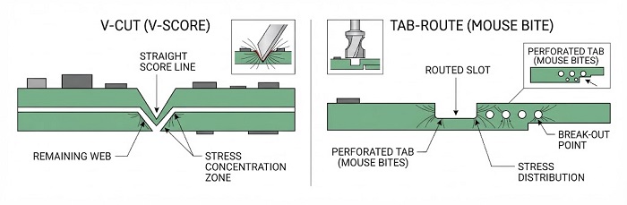
The two most common separation methods differ in throughput, board-shape flexibility, and the mechanical stress they impose on edge components, which makes the choice a real design decision rather than a default.
V-Cut (V-Score)
• Best suited to straight-edge, rectangular boards with no internal cutouts along the score line
• Simpler and typically faster to execute than routing — a straight V-score doesn't require CNC toolpath programming or cutter-wear management the way a routed tab profile does
• Concentrates separation stress along a single straight line, which can transmit flex directly into solder joints and traces close to the score — ceramic chip capacitors and BGA corner balls near a V-score are the most common casualties
Tab-Route (Perforated Tab / Mouse Bite)
• Required for irregular board outlines, internal slots or cutouts, and mixed board shapes combined on the same panel — common in HMLV where a single panel run may need to accommodate more than one job
• Distributes separation stress at discrete tab locations rather than along a continuous line, which allows tab placement to be planned around sensitive components
• Requires clearance planning at each tab break point — for the component body, its solder joints, and the routing tool's own envelope, not just the visible board outline
Decision Logic
V-cut is the reasonable default for simple rectangular boards where minimizing separation time matters most and no components sit close to the panel edge. Tab-route is the safer choice whenever the board outline is irregular, the panel mixes different job designs, or components with flex-sensitive solder joints (connectors, electrolytic capacitors, large BGAs, board-edge mounted parts) are unavoidably close to a break line. In both cases, minimum clearance between components/copper and the separation feature needs to be set in the layout stage — it is not something that can be corrected during final inspection.
Exact edge clearance and spacing requirements vary by assembler and separation method, so confirm the current panel requirements for your build before finalizing the array.
Fiducial and Process Border Design for Placement Accuracy
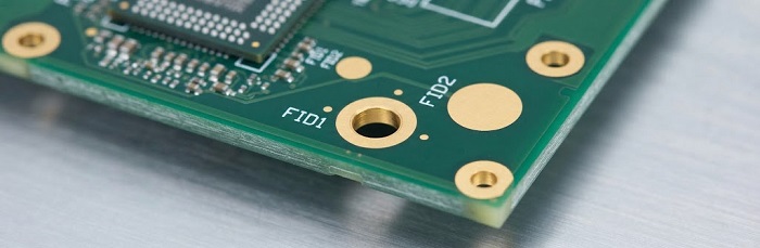
Placement accuracy on a panelized array depends on a layered fiducial scheme, and on a process border designed to keep that scheme readable throughout the line.
• Panel-level (global) fiducials: a minimum of three, arranged asymmetrically so the panel cannot be loaded 180° out of orientation without detection
• Board-level (local) fiducials: typically two to three per individual board, placed on diagonal corners to correct board-level offset and rotation within the panel
• Component-level local fiducials: added adjacent to fine-pitch BGA and QFN packages for local coordinate correction, since panel- and board-level fiducials alone are not tight enough for fine-pitch placement
• Process border / rail: carries fiducials and tooling holes and stays clear of active circuitry, so conveyor clamps and machine vision systems have unobstructed access on the panel's transport edges
This fiducial hierarchy is what our MYCRONIC jet printer and 3D SPI system rely on for paste-print registration and closed-loop correction. If a fiducial is under soldermask, too close to a break line, or placed where a conveyor clamp will cover it during a given process step, the placement or print offset it was meant to catch goes uncorrected — and 3D AOI catches the result downstream instead of preventing it upstream.
Panel Sizing: Reflow Uniformity and SPI/AOI Cycle Time

Panel dimensions affect more than material yield — they influence thermal uniformity through reflow and the inspection cycle time per lot.
• Larger panels can develop a greater temperature delta between the panel center and the rail edges as they move through the reflow oven's zones, which matters most for mixed-thickness HMLV panels running through the JTR-1200D-N
• Thin or large-format panels are more prone to warpage under reflow heat; this is where Synthetic Stone fixtures are used to hold panel flatness and protect BGA/QFN coplanarity on warpage-sensitive boards
• Every panel indexed through 3D SPI and 3D AOI adds a fixed inspection step regardless of panel size, so very small panels multiply the number of indexing cycles per lot, while very large panels increase the inspected area — and potential defect count — per cycle
The practical target is a panel size that keeps thermal profile and warpage within the process window for the specific stack-up and component mix, while keeping the SPI/AOI indexing count reasonable for the lot's target throughput. Off-line X-ray for BGA/QFN voiding is typically staged and indexed the same way SPI/AOI is — at the panel level, before individual boards are separated — so the same panel-size trade-off applies there. Rework access after separation should still be checked at the design stage, not discovered after the fact.
Panelization Design Checklist
• Board count per panel is set against changeover frequency, not maximum material yield alone
• Separation method (V-cut or tab-route) matches the board outline and the sensitivity of edge components
• Minimum clearance is maintained between components/copper and every separation feature
• Panel-level fiducials (≥3, asymmetric) plus board-level and fine-pitch local fiducials are all specified
• Process border/rail is wide enough for tooling holes and clear of conveyor clamp travel
• Panel size has been checked against reflow thermal uniformity for the assigned stack-up
• Panel rigidity and warpage risk have been assessed, with fixture support specified if needed
• SPI/AOI indexing count has been weighed against the lot's target throughput
• Test and rework access after depaneling has been confirmed
Submit Your Gerbers for a Panelization Review
Panelization decisions made at layout are difficult and costly to reverse once the array is in production. If you're finalizing a board design for HMLV assembly, submit your Gerber files for a panelization and DFM review before release — we'll check separation method, fiducial layout, edge clearance, and panel sizing against the process capabilities of the SMT line your job will actually run on.
Helpful Resources
• DFM Audit Checklist for Industrial PCBA: 38 Design Rules That Cut Rework Rate
• BGA Void Rate Acceptance Reference: IPC-7095D & IPC-A-610 Class Criteria
• IPC-A-610 Class 3 Visual Inspection Guide for Industrial & Medical Assemblies


