



High-density switch-mode power supply (SMPS) modules pack power inductors, transformers, MOSFETs, and fine-pitch feedback/control ICs onto increasingly compact boards. From an assembly standpoint, this creates a fundamentally different problem than either pure power boards or pure digital control boards: the same panel now carries components with wildly different thermal mass, standoff height, and pitch tolerance. Getting a high-density SMPS module through SMT and THT processes without compromising either the power stage or the control stage requires deliberate process planning at every station.
Why High-Density SMPS Layouts Are an Assembly Challenge
A typical high-density SMPS module places large-body power inductors or transformers — often several millimeters taller than surrounding components — directly adjacent to 0.4 mm or finer-pitch PWM controllers, current-sense amplifiers, and gate drivers. Two conflicts follow directly from this layout pattern:
Height differential during placement and reflow. Tall power magnetics can shadow adjacent stencil apertures during paste printing and interfere with placement head clearance if package-to-package spacing was not validated against real component height, not just footprint outline.
Pitch conflict at the paste and placement stage. Fine-pitch QFN/BGA control devices sitting close to large discrete power components need independent stencil aperture design (reduced aperture ratios, stepped stencils where justified) so that the print process tuned for power-stage components does not compromise deposition accuracy on the control-stage footprints.
Addressing this starts at DFM review, before the board reaches the line — component keep-out zones around tall magnetics, and stencil design that treats the power and control regions as separate print zones, are the two most effective mitigations available at the design stage.
Reflow Profile Design for Mixed Thermal Mass
The core assembly risk on these boards is thermal, not mechanical: a power inductor or transformer has enough thermal mass that it heats and cools far more slowly than a small-body control IC on the same panel. A single-zone reflow approach tuned to the average component on the board will typically either: under-heat the large-body power components, risking incomplete solder wetting on transformer terminals, or over-heat the smaller, lower-mass control ICs, pushing them toward the upper end of their reflow tolerance and increasing risk to moisture-sensitive or thermally marginal parts.
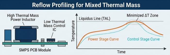
This is where multi-zone reflow profiling is applied deliberately rather than treated as a fixed recipe. On our JTR-1200D-N reflow oven, independent zone temperature setpoints allow the ramp and soak stages to be tuned so that large-mass components reach adequate time-above-liquidus without forcing the smaller control-side components past their peak temperature ceiling. In practice this means:
Profiling is performed with thermocouples placed on both the largest power component and the smallest/most thermally sensitive control IC on the panel, not a single reference point.
Ramp rate and soak duration are set to close the temperature delta between these two extremes as much as the oven's zone count allows, rather than optimizing for either extreme alone.
Profile validation follows standard reflow thermal profiling practice consistent with J-STD-020 classification for the moisture-sensitive devices present on the board.
Boards with an unusually wide component thermal-mass range sometimes also warrant a paste alloy or profile review distinct from the standard board default — this is a design-review-stage decision, not something corrected after the fact on the line.
Selective Wave Soldering for THT Power Terminals
High-density SMPS modules frequently mix SMT control circuitry with through-hole power terminals — heatsink mounting legs, high-current connector pins, or THT power inductors that are not practical to reflow. Standard wave soldering is not viable here, since a full wave pass would expose the adjacent SMD control components to a second thermal excursion and solder wave contact they were not designed to tolerate.
This is the specific use case for automated selective wave soldering. On our ZSWHPS-11-2 selective soldering system, nitrogen-protected localized wave contact is applied only to the defined THT pads — power terminals and heatsink fixing legs — while the surrounding SMD control circuitry, already reflowed, sees no additional thermal or mechanical exposure. Nitrogen protection during the selective pass also reduces oxidation at the solder joint, which matters disproportionately at high-current THT terminals where joint integrity directly affects long-term thermal cycling performance.
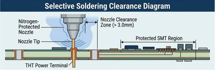
Fixture design matters as much as the soldering parameters here: nozzle programming and pallet design have to account for the proximity of tall power magnetics to the THT pads being soldered, so that the selective pass geometry does not risk contact with adjacent components.
Inspection Strategy: Closed-Loop SPI and AOI
Mixed-technology boards benefit disproportionately from closed-loop inspection, because paste print or placement drift on one side of the board (say, the fine-pitch control region) can be masked in a simple pass/fail AOI check if the overall board yield still looks acceptable.
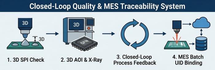
3D SPI measures paste volume, height, and area at each pad immediately after printing — critical on stepped-stencil designs where power and control zones are printed at different aperture ratios, since a print deviation in one zone should not be evaluated against a single board-wide tolerance band.
3D AOI, applied post-placement and post-reflow, catches placement offset and tombstoning risk that is more likely at fine-pitch control footprints located near tall components, where placement head approach angle and post-placement inspection line-of-sight are both more constrained.
Off-line X-ray inspection, with oblique-angle capability, supports BGA and QFN voiding checks on control-side packages — particularly relevant where thermal profiling has been tuned toward the power-side components and control-side solder joint quality needs independent confirmation.
The value of closed-loop SPI/AOI on this board type is specifically that paste and placement data can be fed back into process parameters zone-by-zone, rather than adjusting a single global setting in response to an aggregate yield metric.
MES Traceability for Power Device Root-Cause Analysis
Power semiconductor and magnetic component batch-level traceability is disproportionately important on SMPS assemblies, since field failures in power converters are often thermally or batch-related rather than random defects. Our Smart MES platform, with laser-marked UID at the board or panel level, binds critical power component batch/lot data (MOSFETs, power inductors, control ICs) to the finished unit serial number at the point of assembly.
This traceability structure is what makes root-cause analysis on a field-returned unit actionable rather than speculative — if a failure pattern emerges across a population of fielded units, batch-level data recorded at assembly allows the investigation to start from "which lot, which reflow profile run, which inspection pass" rather than beginning from zero.
DFM Recommendations for High-Density SMPS Assembly
Drawing the above together, the DFM priorities specific to high-density SMPS modules are:
Review component keep-out zones around tall power magnetics against real placement head and post-placement AOI clearance, not just footprint courtyard.
Treat power and control regions of the stencil as independent print zones for aperture design, rather than applying a single stencil thickness/aperture ratio board-wide.
Flag THT power terminals and heatsink legs for selective soldering at the layout stage, with adequate clearance for selective-soldering nozzle access confirmed before fixture design begins.
Specify dual-reference reflow profiling (largest thermal mass component and most thermally sensitive control IC) as a standard DFM checklist item for any board with a wide component thermal-mass range.
Confirm MES traceability requirements — specifically which power components require batch-level UID binding — during NPI planning, not after first article build.
For designs where warpage risk on larger panels compounds the placement-clearance issues above, synthetic stone fixtures used during reflow can help hold panel flatness within the tolerance that fine-pitch placement and AOI inspection depend on.
High-density SMPS assembly is ultimately a coordination problem between two very different component populations sharing one panel — large-mass power magnetics and fine-pitch control circuitry — each with its own placement, thermal, and inspection requirements. Addressing that at the DFM stage, rather than compensating for it after first article, is what determines whether a design reaches production yield on the first pass or requires costly rework cycles. The process decisions outlined here — stencil zoning, dual-reference reflow profiling, selective soldering, closed-loop SPI/AOI, and batch-level MES traceability — are the levers available to make that outcome predictable.
If you're developing a high-density SMPS or power module and want engineering input before committing to a layout or requesting a quote, submit your project for assembly evaluation. Our team will review placement clearance, thermal profiling strategy, and inspection requirements as part of the quoting process.
Helpful Resources
• X-Ray Oblique-Angle Inspection for ATE BGA Boards
• First Pass Yield Improvement Framework for Diagnostic Instrument PCBA
• Stencil Design Requirement on QFN Components for Optimal Performance of PCBA
• Area Ratio Calculation in Solder Paste Stencil Design
• Free DFM Check


