



Industrial and commercial UPS systems, along with the battery chargers that support facility-level power backup, share a design pattern that makes assembly more demanding than a typical single-voltage board: a high-current AC input and rectification stage sits on the same PCB as a low-voltage DC conversion and control stage. Terminal blocks and relays rated for line voltage sit centimeters away from fine-pitch microcontrollers and gate drivers. Getting this combination through assembly reliably means treating the two zones as distinct problems that happen to share a board, a reflow oven, and often a single inspection pass — rather than applying one uniform process across the whole assembly.
This article focuses on stationary and commercial equipment — data center backup UPS units, industrial control-cabinet power supplies, telecom infrastructure chargers, and facility battery banks. It does not address vehicle charging systems, which involve a different set of design and qualification considerations outside this scope.
Isolation and Thermal Zoning on a Mixed-Voltage Board
Two challenges compound on these boards, and both trace back to the same root cause: physical proximity between high-current, line-voltage circuitry and sensitive low-voltage logic.
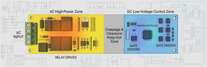
On the isolation side, creepage and clearance requirements around AC input terminals, relay contacts, and rectification components are considerably larger than anything required on the control side. Preserving these distances is not just a layout question — solder mask apertures and paste deposition at the assembly stage can reduce effective creepage below design intent if not checked, and component drift during placement or reflow can erode the margin further. A defined keep-out zone between the AC section and the DC control section needs to be respected through assembly, not just through schematic design.
On the thermal side, AC-side components such as terminal blocks, relays, and high-current fuses carry significantly more thermal mass than the fine-pitch control ICs nearby, yet both pass through the same reflow profile. Multi-zone reflow profiling on equipment like the JTR-1200D-N becomes relevant here — ramp and soak parameters can be tuned so heavier terminal-block and relay joints reach adequate liquidus dwell time without over-stressing the adjacent low-mass control components.
Selective Wave Soldering for AC-Side THT Components
Most mixed AC/DC power boards retain through-hole components on the AC input side — heavy-gauge terminal blocks, power relays, sometimes chassis-mount connectors — because THT still provides better mechanical retention for line-voltage connections exposed to field wiring stress and connector insertion force. These components typically sit within a few centimeters of low-voltage SMD control circuitry that can't tolerate a full wave-soldering pass.
Automated selective wave soldering (ZSWHPS-11-2, nitrogen-protected) directs molten solder only to the defined THT footprint — the AC terminal and relay pads — while the adjacent SMD control area stays outside the solder wave path. Nitrogen protection during the selective pass reduces oxidation and improves wetting on the heavier THT joints, which matters for terminal-block connections that need to hold up mechanically over the equipment's service life. Programming the selective solder pallet and nozzle path for these boards has to account for the same isolation zoning discussed above: fixture design needs to physically shield the DC control area from flux and solder exposure, not just keep the nozzle from making direct contact.
Differentiated Inspection for High-Power and Control Zones
Applying one set of SPI and AOI parameters across a full mixed-voltage board tends to generate false calls somewhere, because solder volume, pad geometry, and acceptable placement tolerance differ substantially between the two sections.
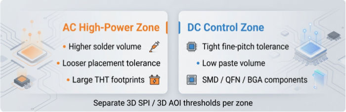
In the AC/high-power zone, SPI thresholds need to account for larger solder volumes on power terminal and relay footprints — a paste height reading calibrated for 0402 passives elsewhere on the board isn't a useful reference here. AOI placement tolerance for through-hole relay and terminal alignment is generally more forgiving than fine-pitch tolerance, since these components tolerate more positional variance without functional impact.
In the DC/control zone, standard fine-pitch inspection practice applies: tighter placement tolerance, paste volume windows suited to smaller apertures, and closed-loop feedback tuned for the control-side component mix. Running these as separately configured inspection zones within a single program — rather than one blanket parameter set — is what makes 3D SPI and 3D AOI closed-loop inspection effective on boards with this level of component diversity. Off-line X-ray with oblique-angle capability remains relevant for any BGA or QFN packages in the control section, particularly for voiding assessment on thermal pads under switching controllers.
MES Traceability for Safety-Critical Components
Fuses, MOVs, and other protective components on UPS and charger boards carry outsized importance relative to their board area, since they're the components most likely to be scrutinized during a field-failure or safety investigation. Lot-level traceability for these specific components — tied through Smart MES with UID traceability and laser marking — allows a manufacturer to identify, for a given serial-numbered unit, exactly which component lot was placed at each safety-critical position.
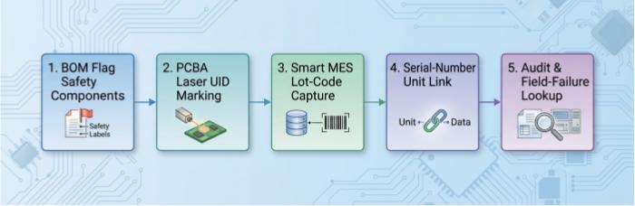
This traceability structure is a manufacturing-record capability that supports internal quality investigation and customer audit requests; it does not constitute a calibration or test-lab accreditation, and boards produced under this process are not represented as having undergone accredited testing.
Design and Assembly Recommendations
Boards in this category benefit from a handful of decisions made before assembly begins: documenting creepage/clearance keep-out zones on the fabrication drawing rather than leaving them implicit in the schematic, specifying THT footprints and fixture-masking requirements explicitly for the selective soldering step, separating SPI/AOI tolerance guidance by zone rather than applying one blanket spec, and flagging safety-critical components for MES lot-tracking at the BOM level before the build starts.
None of these decisions add significant cost or lead time on their own, but skipping any of them tends to surface later — either as an inspection program generating unnecessary false calls, or as a traceability gap discovered only when a field question comes in. Building the zoning, soldering, and inspection strategy into the assembly plan from the start is what keeps a mixed AC/DC power board manufacturable at HMLV volumes without treating each build as a one-off. Teams evaluating a UPS or industrial charger design for outsourced assembly can submit board files for a capability and DFM review to identify these considerations early.
Submit your project for a quote →
Helpful Resources
• X-Ray BGA Void Inspection for Industrial Power Modules
• BGA Void Rate Acceptance Reference: IPC-7095D & IPC-A-610 Class Criteria
• IPC-A-610 Class 3 Visual Inspection Guide for Industrial & Medical Assemblies
• Advanced PCB Assembly Services


