



Chip on Board (COB) assembly — bonding a bare die directly to the substrate and encapsulating it with glob top — addresses a specific set of engineering problems effectively, while introducing constraints elsewhere. For engineers weighing COB against conventional SMT or BGA packaging, the decision generally rests on five practical factors: footprint, cost sensitivity at volume, rework expectations, environmental protection requirements, and the design complexity and timeline a team is prepared to absorb. The sections below examine how each factor weighs for or against COB.
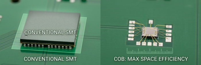
Footprint Constraints
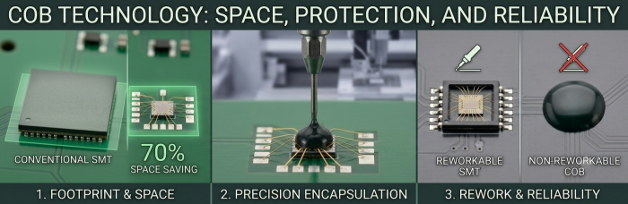
COB eliminates the packaging layer between die and board, so the mounted footprint approaches the size of the die itself. Where board real estate is the binding constraint — wearables, compact sensor modules, handheld instrumentation — this space efficiency is frequently the primary justification for choosing COB over a packaged IC. Where the enclosure allows sufficient room for a standard QFN, BGA, or SOIC footprint, this advantage carries less weight, and the remaining factors become more decisive.
Cost Sensitivity at Production Volume
Bare die is often less expensive per unit than its packaged equivalent, since the cost of the package substrate, leadframe, and molding is avoided. COB, however, requires wire-bonding equipment, die-attach materials, and glob-top dispensing — process steps with their own capital and setup costs that scale differently than die cost alone. At low to moderate volumes, fixed process overhead can offset the savings from bare die. At higher volumes, per-unit packaging savings tend to compound. The determining factor is specific to a given die cost, target volume, and process overhead, and warrants modeling with actual figures rather than an assumption that COB is inherently the lower-cost option.
Rework and Repair Considerations
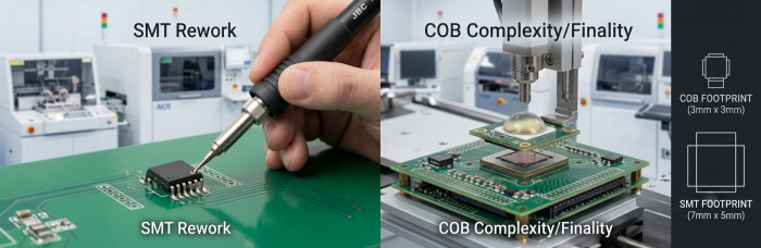
This factor is frequently decisive, and it weighs against COB. Once a die is wire-bonded and encapsulated in glob top, it cannot be reworked in the manner of a packaged component that can be removed and reflowed. A defective die typically results in scrapping the assembly at that location rather than repairing it. Where field serviceability is a requirement, or where die yield is not yet well characterized and rework flexibility is valuable during early production, COB introduces added risk. Where the die is well characterized and the assembly is treated as non-repairable at that level, this concern carries less weight.
Encapsulation and Environmental Protection Requirements
Glob-top encapsulation serves a functional purpose beyond appearance: it protects the bare die and wire bonds from moisture, contaminants, and mechanical stress in the absence of a hermetic package. For products exposed to humidity, vibration, or handling in field conditions, this protection represents a genuine advantage of COB over an exposed die. The advantage is less pronounced where the product already sits within a well-sealed enclosure that provides its own environmental protection, narrowing the marginal benefit of glob top.
Design Complexity and Development Timeline
COB introduces bonding-pad layout rules, wire-bond loop-height and keep-out considerations, and glob-top dispensing patterns not required in a standard packaged-component layout. It also depends on the EMS partner's qualified die-attach and wire-bond capability, and in most cases, an established supply chain for known-good die. Where the timeline is tight and the design team has limited prior experience with bare die, additional design-for-assembly iteration should be anticipated early rather than encountered during DFM review.
When COB Is Not the Right Choice
COB is a poor fit where field repairability is required, where die yield remains unproven and rework flexibility is valuable during early builds, or where board space is not genuinely constrained. In the latter case, a standard packaged component often delivers equivalent performance with simpler sourcing, easier rework, and no dependency on wire-bond processing. COB also warrants reconsideration where an organization lacks an established supply chain for known-good die in the specific part required, since sourcing uncertainty can outweigh the benefits of the packaging approach. In these circumstances, conventional SMT or BGA assembly is generally the more pragmatic choice rather than a compromise.
Weighing the Factors Together
No single factor determines the outcome in isolation. Footprint, cost, repairability, protection, and design readiness need to be evaluated together against the specific product and production volume in question. For teams approaching this decision, reviewing the underlying process and capability details is a reasonable next step.
For engineering teams evaluating COB against alternative packaging approaches, PCBCart's assembly team can review specific design requirements and provide guidance on die-attach, wire-bond, and encapsulation capability. Submit your project details to receive a quote and a capability assessment for your application.
Ressources utiles
• Why Gold Is Essential for PCB Surface Finishes
• PCB Assembly Process - Introduction to PCBA
• Can't-Miss Layout Tips for BGA Chips
• How to Order PCB Assembly Online or Get a Free Quote


