



Outdoor power electronics — PV inverters, energy storage system (ESS) power conversion systems (PCS), and industrial power distribution cabinets — operate in one of the harshest environmental envelopes in electronics manufacturing. Unlike indoor industrial automation boards, these assemblies see daily thermal cycling driven by solar loading and ambient swings, condensation from diurnal humidity shifts, and in many installation sites, salt fog or particulate dust ingress. Protecting the PCBA against this stress matrix is a board-level design and process decision, not an afterthought applied at final assembly.
This article compares conformal coating and potting as protection strategies for stationary, grid-connected power electronics enclosures, and outlines where each approach fits within an HMLV PCBA assembly workflow.
The Environmental Stress Matrix
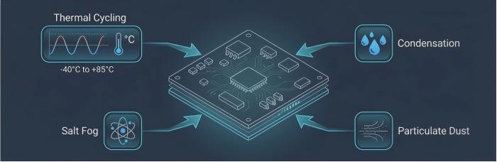
Outdoor power electronics enclosures are typically rated to IP54–IP65 at the enclosure level, but enclosure sealing alone does not eliminate internal stress on the PCBA. Four mechanisms dominate:
Thermal cycling — Diurnal and seasonal temperature swings drive repeated expansion/contraction across solder joints, connector interfaces, and potted/coated boundary layers. Cycle counts over a multi-year service life are substantial even without extreme delta-T per cycle.
Condensation — Enclosures that aren't hermetically sealed experience internal humidity migration; when internal air cools faster than it can vent, moisture condenses directly on the board surface, particularly at conductor edges and under low-standoff components.
Salt spray / fog — Coastal or industrial-adjacent installations introduce chloride ion exposure, which accelerates dendritic growth and electrochemical migration on unprotected conductors.
Dust and particulate ingress — Fine conductive or hygroscopic dust settling on exposed traces can bridge fine-pitch nets over time, especially when combined with condensation.
None of these stresses act in isolation — the design question is which combination of them a given enclosure is exposed to, and how the protective layer needs to respond.
Conformal Coating vs. Potting: Where the Line Sits
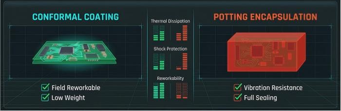
Conformal coating and potting are not interchangeable protection strategies. They sit at different points on a maintainability-versus-protection curve, and the selection should be driven by the board's field service model, not by cost alone.
Conformal Coating — When It Fits
Conformal coating (acrylic, silicone, urethane, or parylene, per IPC-CC-830 material classes) is the appropriate choice when:
The board is expected to be field-serviceable or repairable — coated boards can be selectively stripped and reworked at a connector or component level, whereas potted boards generally cannot.
Vibration exposure is moderate rather than severe (e.g., wall-mounted inverter control boards vs. boards mounted directly on rotating or high-vibration assemblies).
The primary threat is moisture and light particulate, not full immersion or heavy mechanical shock.
Thermal mass and weight are constraints — coating adds negligible mass compared to potting compound.
Potting — When It Fits
Potting (epoxy or polyurethane encapsulation) is the appropriate choice when:
Vibration and mechanical shock are significant — potting compound mechanically stabilizes components and solder joints against fatigue that coating alone cannot arrest.
Contamination exposure is severe — full encapsulation is more resistant to salt fog, conductive dust, and standing condensation than a thin coating film.
The board or sub-assembly is not intended to be field-repaired; potting is, by design, a trade of long-term protection against reduced repairability.
This is the core tradeoff: coating preserves reworkability; potting sacrifices it in exchange for higher environmental robustness. Neither is universally correct — the decision should map to the enclosure's actual field service strategy.
Material Selection and Thermal Resistance Tradeoffs
Within potting specifically, material selection affects more than chemical resistance — it affects the board's thermal path. Thermally conductive (filled) epoxy or polyurethane potting compounds are formulated with ceramic or metal-oxide fillers to reduce thermal resistance relative to standard unfilled epoxy, which is a comparatively poor thermal conductor.
Qualitatively, the tradeoff looks like this:
Standard (unfilled) epoxy potting — Lower material cost, adequate for boards where power dissipation is low or where heat is already managed through a separate heatsink/baseplate path independent of the potting layer.
Thermally conductive (filled) potting — Higher material cost and typically higher viscosity (which affects flow around fine-pitch components), but reduces the thermal resistance added by the potting layer itself — relevant when power devices are encapsulated rather than heatsunk externally.
Exact thermal conductivity values vary significantly by formulation and filler loading; these should be confirmed against the specific compound's datasheet rather than assumed from general potting-material category. For enclosures where power semiconductors dissipate meaningful heat through the potted layer, the material selection decision should be made jointly with the thermal design, not treated as a purely mechanical/moisture-protection choice.
Process Execution: Coating and Potting on the Assembly Floor
Selective Coating Around Connectors and Board Edges
Uniform spray or dip coating is often unsuitable for boards with connectors, test points, or heat sink mounting areas that must remain coating-free. Selective conformal coating using a jetting platform (MYCRONIC jet dispensing) allows programmed, connector-aware coating boundaries — applying coating precisely up to a masked edge without manual mask-and-peel steps. This is particularly relevant on outdoor power boards where connector interfaces (field wiring terminals, RS-485/CAN headers) must stay clean while adjacent low-voltage control circuitry is fully coated.
Vacuum Degassing Before Potting
Potting introduces its own process risk: air entrapment. Voids in cured potting compound create localized weak points — both thermally (air pockets increase local thermal resistance) and mechanically (voids act as crack-initiation sites under thermal cycling). A vacuum degassing step prior to or during potting compound cure is standard practice for eliminating trapped air, particularly around tall components, connector shrouds, and dense component clusters where compound flow is restricted. Skipping this step on complex-geometry boards is a common source of field-observed potting delamination.
Rework Realities: Designing for Serviceability
Potted board rework is, in practice, destructive or near-destructive. Removing cured epoxy or polyurethane potting to access a failed component risks damage to adjacent traces, components, and the board substrate itself — and in most cases, the compound cannot be reapplied to match original coverage and cure integrity. This is a real design constraint, not a process limitation to be engineered around after the fact.
Recommended design-stage mitigations:
Zone the board — Separate high-value, higher-failure-rate components (e.g., control MCU, communication modules) into a non-potted or coating-only zone, reserving full potting for power-stage components with lower expected failure rates.
Modular sub-assembly strategy — Where the enclosure design allows, house potted power sections and serviceable control sections as separate PCBAs connected via board-to-board connectors, so a control-board fault doesn't require potting removal.
Connector-level field service — Design field-replaceable connectors at the boundary between potted and non-potted zones, so troubleshooting can isolate a fault to a replaceable sub-module rather than requiring potting intrusion.
Decision Framework: Coating vs. Potting for Outdoor Power Electronics
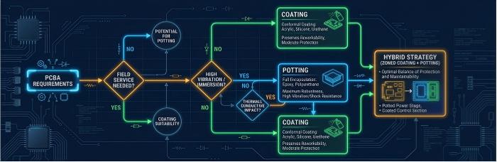
Bringing the tradeoffs together, the selection generally comes down to four questions:
Does the board need to be field-repairable? If yes, conformal coating is the default starting point; potting should only be used on sections the design has already accepted as non-serviceable.
How severe is the vibration and mechanical shock exposure? Low-to-moderate vibration favors coating; high vibration environments favor potting for its mechanical stabilization of solder joints and components.
How severe is the contamination exposure? Moderate moisture and light particulate can typically be managed with coating; severe salt fog, conductive dust, or standing condensation call for potting's full encapsulation.
Does the protective layer sit in the thermal path? If power devices dissipate heat through the potting layer itself, a thermally conductive (filled) compound must be selected — a factor that doesn't apply to thin-film conformal coating.
For many outdoor power electronics enclosures, the practical answer is hybrid: coating on control and communication sub-boards that require ongoing serviceability, and selective potting on power-stage sections exposed to the highest vibration and contamination load.
Getting the Protection Strategy Right the First Time
Choosing between conformal coating and potting isn't a decision that should be finalized in isolation from the rest of the PCBA design — it interacts with thermal management, connector layout, and long-term field service planning. Getting it wrong after tooling and fixtures are committed is expensive to correct, particularly for potted boards where rework options are limited from the outset.
If your outdoor power electronics project — a PV inverter control board, ESS PCS module, or industrial power cabinet assembly — is still in the design or DFM review stage, this is the point where protection strategy should be locked in alongside component placement and thermal path decisions, not added as a final-assembly afterthought.
Submit your outdoor power electronics PCBA project for an engineering review covering conformal coating vs. potting selection, thermal path impact, and field-serviceability zoning — before your design moves into tooling.
Helpful Resources
• Why Do PCBA Vias Fail During Thermal Cycling?
• Comprehensive Guidelines for Design, Materials, and Components in High-Performance Power Electronics PCBs
• Waterproof PCBs: Design Guide & Protection Methods
• X-Ray BGA Void Inspection for Industrial Power Modules
• Top 10 Applications for PCBs


