



A design that passes schematic review can still fail on the line. DFM/DFA issues — a footprint mismatched to the paste stencil, a test point buried under a connector, a selective-solder keepout never drawn — are cheap to fix on a CAD screen and expensive to fix after first-article build. This checklist gives engineering teams a structured, 42-point pre-production audit across six categories, focused on industrial automation and life sciences hardware where field failures carry outsized cost and traceability is non-negotiable.

This is an assembly-side (PCBA) checklist. It assumes the bare board is already fabricated and verified separately — it does not cover fabrication-level DFM (stackup, copper weight tolerancing, etc.).
How to Use This Checklist
Run it at three gates: schematic freeze, layout freeze, and the final Gerber/BOM package before kickoff. Each item is binary pass/fail — no partial credit — to keep the audit fast and remove subjective judgment from a process that should be deterministic.
1. Pad Design & Spacing (10 items)
Footprints match manufacturer land-pattern recommendations, not just the datasheet outline
Minimum pad-to-pad spacing supports the smallest passive package in the BOM
Fine-pitch (≤0.5mm) pads called out as solder-mask-defined (SMD) or non-solder-mask-defined (NSMD)
Thermal/exposed-pad vias sized and tented/plugged to prevent paste wicking during reflow
No copper slivers or overly acute-angle pad geometry that risks etch/print defects
Fiducials present at panel and local component level for fine-pitch parts
Panelization break-tabs do not intersect pads or clearance zones
BGA/QFN ball pitch confirmed against the stencil aperture plan, not assumed from datasheet
Edge-of-board clearance respects the depanelization method (V-score vs. routed)
Safety/creepage clearance between high- and low-voltage nets meets the spacing standard for the stated working voltage and pollution degree
2. Stencil & Solder Paste Design (7 items)
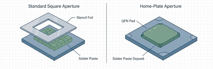
Stencil thickness matched to the finest-pitch component, not a single board-wide default
Aperture reduction ratios calculated for fine-pitch QFN/BGA to control paste volume
Home-plate or window-pane apertures specified for large thermal pads to allow outgassing and reduce voiding
Step-stencil requirements flagged where mixed component heights need differential paste deposit
Jet-printing/dispensing flagged as the paste-deposit method where stencil printing is impractical (e.g., low-volume mixed-lot runs)
Two-pad passive footprints (chip resistors/capacitors) checked for symmetric aperture sizing to avoid solder-volume imbalance and tombstoning
Stencil/frame design compatible with automated cleaning cycles
3. Wave/Selective Soldering Process Zone (6 items)
Through-hole and SMD zones clearly separated — no SMD parts inside the selective-solder pallet travel path
Adequate shadowing clearance around tall components adjacent to through-hole pins
Solder-side component orientation minimizes bridging risk (pin rows parallel to wave direction where applicable)
Nitrogen-protected selective soldering specified for lead-free through-hole joints on dense boards to control dross and bridging
No SMD components inside the minimum keepout distance of any through-hole pad scheduled for selective soldering
Fixture/pallet cutout locations defined in CAD, not left for the assembly floor to improvise
4. Test Points & ICT Accessibility (8 items)
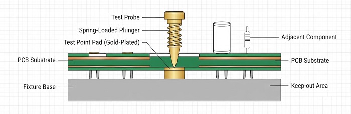
Every net requiring ICT coverage has a dedicated, probe-accessible test point — not a via reused as a probe pad
Test points on both sides where single-sided fixturing isn't feasible
Minimum test point diameter and pitch confirmed against the fixture probe spec, not assumed
No test points under connectors, heatsinks, or tall components after final assembly
Power and ground test points isolated from noisy switching nets
Boundary-scan (JTAG) access points identified for BGA-heavy designs where physical probing isn't possible
Test point placement checked against panel breakout — points stay accessible if ICT runs pre-depanelization
Fixture nest clearance confirmed for tallest component plus expected board warpage
5. Thermal Management & Component Orientation (6 items)
Copper pour and thermal relief pattern checked for uniform heat distribution — asymmetric copper density near high-mass components is a common root cause of uneven reflow and cold joints
Reflow profile compatibility (JTR-1200D-N oven) confirmed against the largest thermal-mass component, not the board average
Polarized components (diodes, electrolytic caps, ICs) have silkscreen orientation marks that survive reflow and stay visible for AOI verification
Component placement avoids thermal shadowing where large parts block reflow airflow to adjacent fine-pitch devices
Warpage-sensitive assemblies (thin panels, large BGA count) flagged for fixture-assisted reflow (synthetic stone fixtures) rather than free-floating conveyor transport
Keep-out zones defined around heat-generating components to prevent coupling to temperature-sensitive parts
6. Life Sciences & Industrial Special Requirements (5 items)
Cleaning compatibility confirmed for any conformal-coating or cleanroom-adjacent build — flux chemistry and post-solder cleanliness defined before kickoff, not discovered at inspection
Pad and clearance dimensions reviewed against IPC Class 3 where the application calls for high-reliability acceptance criteria
Component orientation and lot-traceability marking requirements documented per device, not assumed to be "standard silkscreen"
Safety/creepage clearance sign-off is documented against the specific standard named in the design spec — not left as an unwritten assumption carried over from a prior program
Voiding acceptance criteria for BGA/QFN thermal and power pads defined in writing before build, not negotiated after X-ray results come back
A note on scope: we assemble to IATF 16949-certified process controls. We do not hold ISO 13485 certification. If your program requires ISO 13485-certified assembly as a contractual gate, resolve that with your quality team before kickoff — we can build to IPC Class 3 and document the requirements above, but we are not representing ISO 13485 medical-device QMS certification.
Where the Real Risk Concentrates

Three failure modes account for a disproportionate share of first-article rejects on industrial boards:
Uneven copper thermal mass. A dense ground plane on one side and sparse routing on the other reflows unevenly, producing cold joints right at the connector or power stage. This is a layout item, not a reflow-profile item — profile tuning can't fully compensate for a copper-density imbalance baked into the design.
Insufficient safety/creepage clearance. Designers often apply one clearance rule across the whole board instead of re-checking it per voltage domain and pollution-degree assumption. On mixed-voltage industrial boards this is the most common single item to fail a DFM review.
Selective-solder keepout violations. SMD parts placed too close to through-hole pads scheduled for selective soldering get exposed to solder splash or thermal shock they weren't designed for — often surfacing as intermittent field failures months later rather than an obvious first-article defect.
Using This Checklist to Evaluate a Contract Manufacturer's DFM Capability
Not every assembly partner reviews all 42 points as routine process. When qualifying a supplier, ask them to walk your board through this checklist and show where each check happens — schematic, layout, or Gerber/CAM review — and with what tooling. 3D SPI/AOI and X-ray voiding analysis are reasonable evidence for the thermal and stencil categories; MES-based traceability and laser marking are reasonable evidence for the life-sciences category.
As a rule of thumb: a supplier whose standard DFM process covers fewer than 30 of these 42 items is running a Gerber sanity check, not a capability-level DFM audit. That distinction matters most on dense industrial power/control assemblies and life-sciences instrumentation, where a missed clearance or unmarked polarity isn't a yield statistic — it's a field return.
Get This as a Working Document
This checklist is available as a static, printable PDF form with checkboxes — a fillable form, not a web app — so your team can print it, mark it up during design review, or fill it in any PDF viewer with no dev resources or software integration required.
To have your own design reviewed against it: upload your Gerber/ODB++ package and BOM for a DFM audit. We'll check the file set against this checklist and our assembly process — Automated Selective Wave Soldering with N2 protection, MYCRONIC jet-print/dispense, 3D SPI + 3D AOI closed-loop inspection, off-line X-ray voiding analysis, and Smart MES UID traceability — and flag any of the 42 points that don't clear. We aim for prompt feedback; confirm current turnaround with your account contact when you submit.
Helpful Resources
• Effective Measures for Quality Control on BGA Solder Joints
• Common SMT Defects and How to Avoid Them
• IPC-A-610 Class 3 Standards for Life Sciences Electronics
• PCBCart's Advanced PCB Assembly Capabilities


