



Many first-article problems on industrial wireless boards are not RF design errors but manufacturability gaps: a shield frame starved of paste, a module ground pad with too few vias, an antenna keep-out that never reached the coating drawing. This checklist catches them before Gerber release.
It is an RF-specific supplement to our general 42-point PCBA DFM/DFA checklist, with 31 checks in five categories, each with a reference basis and the typical consequence of a violation. In the Owner column, A items can be verified by the assembler from your files and build records; D items are design decisions only your team can confirm.
The Checklist
1. Shielding & Grounding (8 items)
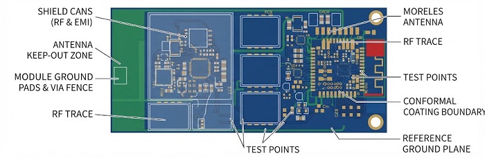
| # | Owner | Check | Reference basis | Consequence if violated |
|---|---|---|---|---|
| 1.1 | A | Shield frame/clip land pattern matches the shield vendor drawing | Shield vendor drawing; IPC-7351 | Frame skew; gaps that leak RF |
| 1.2 | A | Frame stencil apertures segmented and sized for area ratio and paste volume | IPC-7525 (area ratio ≥0.66 guideline) | Open or starved joints along frame edges |
| 1.3 | D | Shield ground ring stitched to reference ground with a via fence | IPC-2252; rule of thumb: pitch ≤λ/20 at top frequency | Slot leakage, reduced isolation |
| 1.4 | A | Vias in or near shield pads tented, plugged, or offset | IPC-4761 | Solder wicking, weak fillets |
| 1.5 | A | Tallest part under the can clears the lid height | Shield drawing; component datasheets | Lid contact, shorts, detuning |
| 1.6 | D | One- vs. two-piece can chosen for rework access | IPC-7711/7721 | Scrap when shielded parts need rework |
| 1.7 | D | Unbroken ground reference under RF traces and module | IPC-2252 | Impedance discontinuity, emissions |
| 1.8 | A | Reflow profile accounts for can thermal mass | IPC-7530; paste vendor profile | Cold joints at frame corners |
2. Antenna Clearance & Routing (7 items)
| # | Owner | Check | Reference basis | Consequence if violated |
|---|---|---|---|---|
| 2.1 | D | Antenna keep-out copper-free on all layers per datasheet | Module/antenna integration guide | Detuning, range loss |
| 2.2 | A | No components, standoffs, or metal hardware inside the drawn keep-out | Integration guide | Pattern distortion |
| 2.3 | D | Antenna placement matches the module's certified reference layout | Integration guide; FCC KDB 996369 | Modular approval may not apply; re-test |
| 2.4 | D | RF feed impedance controlled; stackup stated on fab drawing | IPC-2141; IPC-2252 | Mismatch, lower radiated power |
| 2.5 | D | Matching network placed at the feed; populate/DNP state explicit in BOM | Antenna vendor app notes | Board built untuned |
| 2.6 | A | Silkscreen, labels, and UID laser marks kept out of the antenna area | Integration guide | Mark relocation after first article |
| 2.7 | A | U.FL/SMA footprint and ground clearance per connector datasheet | Connector datasheet | Impedance step, intermittent mating |
3. Module Assembly Compatibility (6 items)
| # | Owner | Check | Reference basis | Consequence if violated |
|---|---|---|---|---|
| 3.1 | A | Module land pattern taken from the module datasheet, not a generic LGA | Module datasheet; IPC-7093 | Opens, bridging |
| 3.2 | A | Center ground pad paste window-paned (segmented) | IPC-7093; IPC-7525 | Module float, tilt, voiding |
| 3.3 | A | Ground via count under the module meets the datasheet; vias plugged/tented | IPC-7093; IPC-4761 | Weak RF/thermal ground, voids |
| 3.4 | A | Moisture sensitivity level stated; bake and floor-life plan defined | J-STD-033 | Delamination, popcorning |
| 3.5 | A | Module coplanarity reviewed against board warpage | Module datasheet; IPC-7093 | Corner opens |
| 3.6 | D | Void acceptance criteria for the module ground pad defined on the drawing | IPC-A-610; IPC-7093 | Accept/reject disputes |
4. Test Points & RF Test Access (5 items)
| # | Owner | Check | Reference basis | Consequence if violated |
|---|---|---|---|---|
| 4.1 | D | Conducted RF test path designed in (switch connector or 0 Ω diversion) | Module/antenna vendor guidance | Radiated-only testing, slow debug |
| 4.2 | A | No test points inside the antenna keep-out or under shield lids | Integration guide | Can removal needed to probe |
| 4.3 | D | Shielded nets brought out to pads outside the can | IPC-2221 (testability) | Untestable inner nets |
| 4.4 | A | Test pad size and spacing suit fixture probing | IPC-2221; fixture vendor rules | Probe skid, component damage |
| 4.5 | A | Programming interface reachable after shielding and coating | Design spec | Rework to load firmware |
5. Conformal Coating Keep-Out Marking (5 items)
| # | Owner | Check | Reference basis | Consequence if violated |
|---|---|---|---|---|
| 5.1 | D | Radiator defined as keep-out, or coating effect characterized | IPC-HDBK-830; antenna vendor | Resonance shift |
| 5.2 | A | RF connector mating surfaces masked | IPC-HDBK-830 | Mating failure |
| 5.3 | A | Shield lid clip interfaces and test points masked | IPC-HDBK-830 | Lid won't seat; test contact fails |
| 5.4 | D | Keep-outs drawn on a dedicated, dimensioned layer, not only in notes | IPC-HDBK-830; drawing practice | Operator interpretation errors |
| 5.5 | D | Coating material type and thickness range specified | IPC-CC-830; IPC-A-610 | Uncontrolled thickness, RF drift |
High-Risk Items in Industrial Wireless Builds
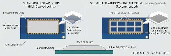
Shield-can stencil apertures too small → open or starved joints
Stencil thickness is usually set by the finest-pitch parts, so narrow shield-frame pads can receive too little paste. Any coplanarity error then becomes corner and mid-span opens that may pass functional test while leaking RF.
• Design side: segment the frame aperture instead of one continuous slot, sized against the IPC-7525 area-ratio guideline; use a step stencil only where volume is still short.
• Process side: 3D SPI measures paste volume along the full frame, and a MYCRONIC jet printer can add localized paste where a stencil change is impractical. After reflow, inspection concentrates on the four corners, with X-ray where the can body hides the joint.
The full shield-can stencil, placement, and post-reflow verification sequence is covered separately.
Antenna area coated by mistake
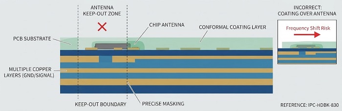
The keep-out often lives only in the module datasheet, while the coating program is built from the board outline. Coating adds dielectric around the radiator and can shift its resonant frequency; the size of the shift depends on material and thickness, so item 5.1 allows characterization instead of a blanket ban.
• Draw the keep-out on its own dimensioned layer and reference it on the coating drawing, as in our conformal coating strategies for industrial IoT gateway boards.
• Verify masking on the first article before releasing the coating program.
Too few ground vias under the module
Too few vias raise ground inductance and weaken heat spreading. Open vias in the pad also wick solder and let trapped gas into the joint, increasing voids under the LGA ground pad.
• Match via count and pattern to the module datasheet, and specify plugged or capped vias per IPC-4761.
• Window-pane the ground-pad paste, then inspect with off-line X-ray against agreed void criteria, using oblique angles where the module body obscures the joint. See ground-pad void control on cellular and LoRa modules.
Using the Checklist to Evaluate a Supplier's RF Assembly Capability
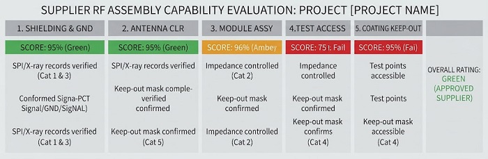
Send the checklist with your design package and ask each supplier to mark how each item is covered — automated file check, engineer review, or not at all — then score each category red/amber/green.
• Categories 1 and 3: can they show first-article SPI volume records and X-ray images for the shield frame and module ground pad?
• Category 5: how is the keep-out turned into masking or a selective program, and verified?
• Traceability: is each module's lot/date code bound to the board serial number? At PCBCart, Smart MES records it against a laser-marked UID at placement.
• Test scope: ask who performs RF performance testing. PCBCart is IATF 16949 certified but holds no RF/EMC test-lab or calibration accreditation, so conducted and radiated RF testing stays with your team or test house — write that into the build package.
A supplier that marks every item "covered" without saying how tells you less than one that hands the D items back to you.
Get the Printable Checklist and a DFM Pre-Review
This checklist is available as a static, printable PDF form — Pass / Fail / N/A boxes per item, a notes column, and reviewer sign-off. Print it or annotate it in any PDF reader.
Next step: submit your Gerber files, BOM, module datasheet, and coating drawing for an RF/wireless DFM pre-review. Our Free DFM Check runs automated file-level checks, including defined keep-out areas; our engineers then flag assembly-side risks on the A items before first article. RF performance, antenna tuning, and certification remain with your design team.
Helpful Resources
• Antenna Design Considerations in IoT Design
• Grid-Tie Inverter Communication Board Assembly: EMI/EMC-Aware PCBA Practices


