



Automated test equipment (ATE) boards present a distinct set of new product introduction (NPI) requirements for low-volume, high-mix semiconductor manufacturing. Load boards, device interface boards (DIB), probe interface boards, and burn-in boards are rarely subject to a single linear qualification path. Design revisions are dictated by device tape-out schedules, socket footprints change between engineering sample cycles, and production volumes remain low even once a board has been formally qualified. For an HMLV (High-Mix, Low-Volume) PCBA manufacturing partner, this places a distinct requirement on the NPI process itself: it must be structured around iteration and full traceability, rather than around ramping a single design toward high-volume steady-state production.
This article presents a stage-gated NPI process for ATE board manufacturing, addressing how inspection data progressively tightens process tolerances, how changeover efficiency governs NPI cycle time in a high-mix production environment, and how yield and coplanarity data from the qualification run function as the methodological gate for production release.
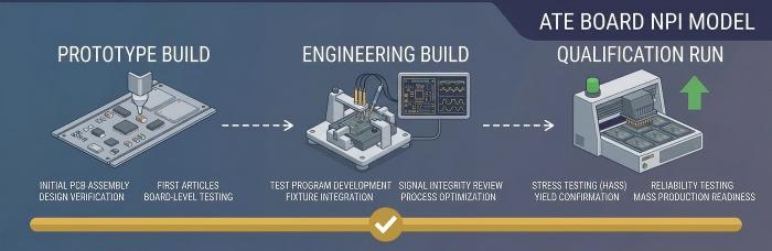
Why ATE Board NPI Departs From a Standard PCBA Framework
Conventional PCBA NPI models generally assume that a design will eventually transition to volume production, allowing early-stage inspection cost to be amortized across a longer production run. ATE board manufacturing departs from this assumption in two structural respects:
Production volume remains flat. A DIB engineered for a specific device package may require only tens to low hundreds of units across its entire production life. With no subsequent high-volume phase to average against, process capability must be established and proven at low unit counts.
Mechanical tolerance requirements are front-loaded. Coplanarity, socket seating force, and BGA/pogo-pin pad alignment—parameters that would be secondary considerations on a general industrial board—constitute functional requirements on an ATE board, as they directly govern device contact integrity and downstream test yield at the customer's test cell.
This distinction reframes the purpose of the prototype stage. Rather than serving solely to validate the design, it establishes the process window that the subsequent qualification run is required to hold.
Stage 1: Prototype Build
Objective: Confirm assembly feasibility and identify design-for-manufacturing (DFM) risks prior to committing to production fixturing.
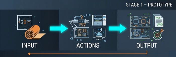
Prototype builds typically involve low unit counts—single-digit to low double-digit quantities—with emphasis placed on identifying mechanical and process risk rather than establishing statistical process control.
Core activities at this stage include:
Solder paste deposition review. For boards combining fine-pitch BGA with coarser-pitch connectors, MYCRONIC jet printing/dispensing accommodates paste volume variation across a single board, avoiding the tooling lead time associated with a dedicated stencil at this early stage.
First-article 3D SPI. Solder paste height and volume are verified pad-by-pad against nominal specification, primarily to identify print process deviations—bridging risk or insufficient volume on large BGA balls—prior to reflow.
Post-reflow 3D AOI. Component placement, polarity, and solder joint geometry are inspected across 100% of prototype units, as sample sizes at this stage are insufficient to justify sampling-based inspection.
Off-line X-ray inspection on BGA/QFN sites. Voiding is assessed across all ball-grid and leadless package sites. This carries elevated significance for ATE boards, as voiding beneath socket-mounted BGAs can interact with mechanical seating stress in ways not detectable through external inspection alone.
Warpage verification using synthetic stone fixtures. Boards are seated on synthetic stone reference fixtures to assess flatness—a parameter of disproportionate importance for boards that will subsequently mate with a precision test socket or pogo-pin interface.
Findings from this stage are typically fed back into stencil design, paste profile parameters, or component placement decisions, rather than into finalized process settings.
Stage 2: Engineering Build (Pilot Run)
Objective: Lock the process window based on prototype-stage data, and begin narrowing inspection tolerances toward the qualification run's acceptance criteria.
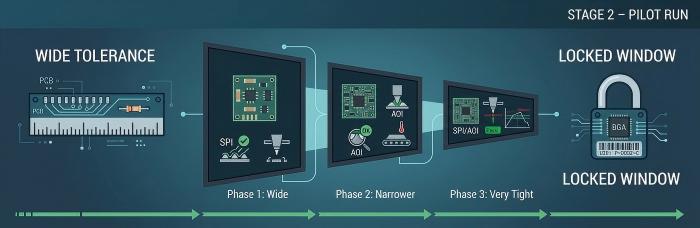
The engineering build occupies the interval between prototype and qualification, executed in batch sizes sufficient to observe process repeatability rather than a single first article. Tolerance bands are progressively narrowed at this stage:
SPI acceptance windows are tightened. Paste volume tolerances, deliberately held wide during the prototype stage to characterize the full process range, are narrowed toward the target band once pilot-stage data establishes where the process centers.
AOI defect libraries are refined. False-call patterns identified during the prototype build inform adjustments to AOI algorithm thresholds specific to the board's component mix, reducing inspection noise ahead of the qualification run's go/no-go decision.
Selective soldering parameters are finalized. For boards incorporating through-hole connectors adjacent to dense SMT areas—common on DIB and probe-interface boards—the ZSWHPS-11-2 selective wave soldering system, operated under nitrogen protection, is used to finalize preheat and dwell parameters without exposing adjacent fine-pitch SMT components to thermal risk.
Reflow profile finalization on the JTR-1200D-N. Profiles are locked based on thermocouple data collected from pilot units, accounting for the thermal mass characteristic of ATE boards, which frequently carry heavier connectors and heat-sinked components than a typical control board.
Every unit remains tracked individually through Smart MES with UID-level traceability and laser marking, enabling any downstream issue observed at the customer's test cell to be traced to its specific paste lot, reflow cycle, and inspection record—a requirement of particular consequence for ATE boards, given the direct relationship between assembly variation and test measurement integrity.
Stage 3: Qualification Run — Yield and Coplanarity as the Production Gate
Objective: Demonstrate that the locked process performs consistently at a batch size sufficient to be statistically meaningful, rather than relying on isolated results.
The qualification run marks the transition from confirming that a build succeeded to confirming that a process is repeatable. Two data sets are methodologically central to this determination:
First-pass yield across the qualification batch, tracked at both the SPI and post-reflow AOI stages. Rather than evaluating a single pass/fail outcome, the qualification run assesses stability across the full batch—consistent centering within tolerance bands, not merely individual unit compliance.
Coplanarity data across the batch, referenced against the synthetic stone fixture baseline established during the prototype stage. For socket-mounted or pogo-pin-interfacing boards, coplanarity consistency across the qualification batch serves as a leading indicator of field-level test yield at the customer's ATE cell, given its direct bearing on contact reliability.
Only once these data sets confirm that the process holds within the tightened Stage 2 tolerance bands does the design advance to production-release status. This represents a methodological standard rather than a fixed numeric benchmark—specific acceptance thresholds are established per program, based on the board's functional requirements and the customer's own test yield targets.
Changeover Efficiency and Its Effect on NPI Cycle Time
Within an HMLV production environment, ATE board NPI seldom proceeds in isolation. A given line may concurrently run a qualification build for one program alongside a prototype build for another. Changeover efficiency between these jobs materially governs how rapidly an NPI program can progress through its stages:
MYCRONIC jet printing eliminates stencil-related changeover delays between prototype iterations, as paste deposition parameters can be reprogrammed rather than requiring new tooling for each design revision.
MES-driven program recall on AOI/SPI and reflow equipment reduces setup time as a line alternates between an NPI build and unrelated production jobs, since inspection algorithms and thermal profiles are retrieved by program ID rather than re-entered manually.
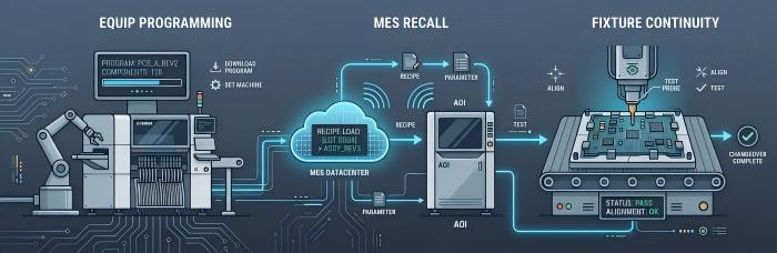
Fixture continuity across stages. Retaining the same synthetic stone fixture family from prototype through qualification—rather than switching fixture types between stages—preserves coplanarity baseline consistency and avoids re-characterization time.
Where changeover efficiency is deficient, the resulting cost typically manifests as elapsed calendar time between NPI stages rather than as unit cost—a consequence of particular significance for ATE board programs, where the interval between device tape-out and test readiness often affords little schedule margin.
NPI Stage-Gate Checklist
Prototype build: Feasibility confirmed via 100% AOI/X-ray inspection; DFM issues documented; warpage baseline established on synthetic stone fixtures.
Engineering build: SPI/AOI tolerance windows tightened using prototype-stage data; selective soldering and reflow parameters locked; UID-level traceability active for every unit.
Qualification run: Batch-level yield and coplanarity data reviewed against tightened tolerance bands; process stability—not single-unit pass/fail—confirmed prior to production release.
Production release gate: Documented process window, inspection acceptance criteria, and MES program lock-in finalized and archived for future production re-runs.
From Prototype to Production-Ready: Consult Our NPI Engineering Team
Programs advancing an ATE, burn-in, or DIB board from prototype toward a qualification run benefit from stage-gate planning specific to the board's tolerance, coplanarity, and traceability requirements. PCBCart's engineering team supports this planning directly, drawing on inspection-driven process development across semiconductor test board programs.
Helpful Resources
• DFM Audit Checklist for Industrial PCBA: 38 Design Rules That Cut Rework Rate by Over 40%
• IPC-A-610 Class 3 Visual Inspection Guide for Industrial & Medical Assemblies
• BGA Void Rate Acceptance Reference: IPC-7095D & IPC-A-610 Class Criteria
• Elements Ensuring Your First-Time Success in New Product Introduction (NPI) during Electronic Manufacturing


