



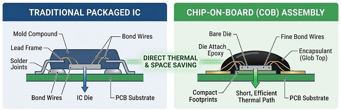
Chip-on-board (COB) assembly mounts a bare die directly on the substrate, connects it with fine bond wires, and seals it under an encapsulant. Sensor designers choose COB mainly because it removes the package: the module gets smaller, the thermal path gets shorter, and the sensing element sits closer to what it measures. The tradeoff is that work normally done at a packaging house now happens on your board. Each step must be verified before the next one buries it.
This guide covers the engineering decisions that matter most in COB sensor module manufacturing: bond selection, bond-strength verification, encapsulation, inspection limits, and design for manufacturability (DFM).
Why Sensor Modules Use Chip-on-Board
A packaged IC places a lead frame or laminate, mold compound, and solder joints between the die and the PCB. COB removes most of those layers, which gives sensor modules three advantages:
Smaller footprint and lower profile. The module is roughly the die plus wire fan-out and an encapsulant margin. This matters in probe tips, compact instruments, and dense sensor arrays.
Tighter thermal coupling. The die-attach layer becomes the main thermal interface, so temperature-sensing dies track board temperature more closely.
Direct sensing access. Optical, pressure, and MEMS dies can stay partly exposed, or sit under a window or lid instead of being fully molded.
The cost is a tighter process window. Bond pads must stay free of contamination. Die placement must stay within reach of the bonding tool. Board flatness affects loop consistency. Bare die also needs stricter ESD handling than packaged parts. Finally, overall yield equals assembly yield multiplied by the yield of the incoming die, and bare die typically carries less test coverage than packaged devices.
Wire Bonding Fundamentals for Sensor Modules
This section assumes familiarity with die attach and focuses on the bonding choices that matter for wire bonding PCBA in sensor applications.
Gold Ball vs. Aluminum Wedge Bonding
Two processes cover nearly all COB sensor work:
Gold ball bonding (thermosonic) combines heat, ultrasonic energy, and force. It is fast and can route wire in any direction after the first bond, which suits high-I/O dies. It requires a bondable gold surface on the board, typically ENEPIG or electrolytic soft gold. Standard ENIG gold is generally considered too thin for reliable gold ball bonding.
Aluminum wedge bonding (ultrasonic) runs at room temperature. It suits heat-sensitive substrates and forms a single-metal (monometallic) bond on aluminum die pads. It is slower, because the tool must align with each wire’s direction.
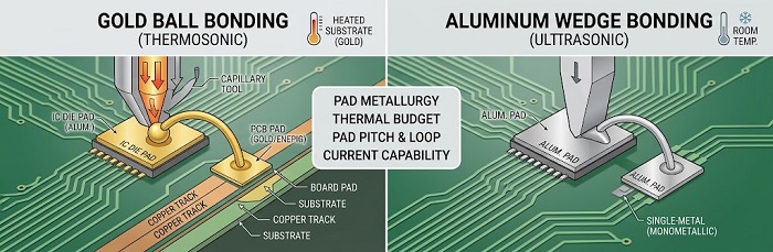
Four factors drive the choice:
Pad metallurgy. Gold wire on aluminum pads forms Au–Al intermetallics. At sustained high temperatures these can grow and develop Kirkendall voids, a real risk for high-temperature industrial sensors.
Thermal budget. If the substrate or nearby components cannot tolerate the bonding stage temperature, choose aluminum wedge.
Pad pitch and loop shape. Ball bonding generally reaches finer pitch and offers more freedom in loop shape.
Current. Heavier aluminum wire is used where the die carries significant current.
Verifying Bond Strength
Bond strength must be measured, not judged by appearance. Three methods are standard:
Destructive wire pull test (MIL-STD-883, Method 2011). This standard tabulates minimum pull forces by wire material and diameter. Record the failure mode as well as the force: neck break, heel break, mid-span break, or lift at the bond. An interface lift points to a marginal process, even when the force value passes.
Non-destructive pull test (MIL-STD-883, Method 2023). It applies a fixed force to every wire and is used where 100% screening is justified.
Ball shear test (JEDEC JESD22-B116). It evaluates the ball-to-pad bond, which a pull test does not measure directly.
Run destructive samples at setup, after every parameter change, and at a defined frequency during production. Document the sampling plan in the control plan.
Glob Top Encapsulation: Materials and Process Controls
Glob top protects the wires mechanically and keeps moisture and ionic contamination away from the die. It is also where many reliability problems begin. Selection follows much of the same logic as conformal coating, with tighter constraints because the material touches unsupported wires.
Key material properties:
Tg relative to operating temperature. Above Tg, CTE rises sharply and stress on the wires increases.
CTE and filler content. Filled epoxies reduce the expansion mismatch with the die and wires.
Modulus. Silicones are low-stress and suit MEMS and pressure dies, but they offer less mechanical protection and absorb more moisture.
Ionic purity. Low chloride and sodium content limits corrosion of aluminum pads.
Cure shrinkage and moisture uptake. Both add stress to bond wires over the module’s life.
Key process controls:
Dam-and-fill vs. single glob. A thixotropic dam defines the footprint and a low-viscosity fill flows around the wires. This controls height and edges better than a single dispense.
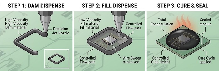
Dispense temperature, viscosity, and flow path. These determine wire sweep. Fill from the side away from the longest wires.
Pre-bake and degassing. Removing moisture from the board and air from the resin prevents voids.
Staged cure. Gradual ramps reduce shrinkage stress and keep trapped gas from expanding.
PCBCart’s MYCRONIC jet printer/dispenser provides programmable, non-contact deposition. Whether a specific dam or fill material can be jetted depends on its rheology and must be qualified material by material.
How Reliability Requirements Differ Across Three Industries
Industrial Sensor Modules
Wide temperature cycling, vibration, humidity, and possible chemical exposure dominate. Priorities are intermetallic stability at temperature, an encapsulant Tg well above the operating ceiling, and loop shapes that resist vibration fatigue. Monitoring sensors in stationary inverters, grid equipment, and UPS systems also face sustained heat from nearby power stages.
Medical Diagnostic Sensors
PCBCart does not hold ISO 13485 certification. For COB modules used in diagnostic instruments, the engineering priorities are cleanliness, low ionic residue, stable sensor offset after encapsulation, and lot-level traceability for die, wire, and encapsulant. Encapsulation stress can shift sensor offset, so module-level calibration and test should run after cure. Teams whose regulatory pathway requires an ISO 13485-certified supplier should factor that into scope decisions.
Semiconductor Test Equipment Modules
Sensor modules in test equipment cycle repeatedly across test temperatures and often sit near low-current measurement paths. Priorities are low surface leakage, ionic cleanliness, low-outgassing encapsulants for enclosed thermal chambers, and flatness where modules mate mechanically with probe interfaces.
What Inspection Can—and Cannot—Confirm
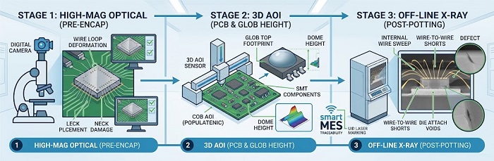
No single inspection method covers a COB module. Each stage needs its own check:
High-magnification optical inspection before encapsulation. MIL-STD-883 Method 2010 defines internal visual criteria for bond deformation, placement, loop height, neck damage, and wire-to-wire clearance. Defects missed at this stage cannot be found later.
3D AOI is built for solder joints, not wire loops in the 25 µm class, and should not be presented as wire bond inspection. In COB flows it confirms die presence, position, and rotation. It also measures glob top footprint and dome height from 3D profiles and checks the surrounding SMT. Upstream, 3D SPI confirms that no solder paste was printed near bond-pad areas.
Off-line X-ray sees through cured encapsulant. Gold wire shows high contrast, so wire sweep and shorts can be checked after potting. Oblique-angle imaging separates overlapping loops. Aluminum wire has poor X-ray contrast, which limits this method for wedge-bonded modules. X-ray also measures voiding in solder or silver-filled die attach.
Smart MES with UID laser marking links each module serial number to the material lots recorded at every step. Die-level traceability depends on bare die being received and logged by lot.
DFM Checklist for COB Sensor Modules
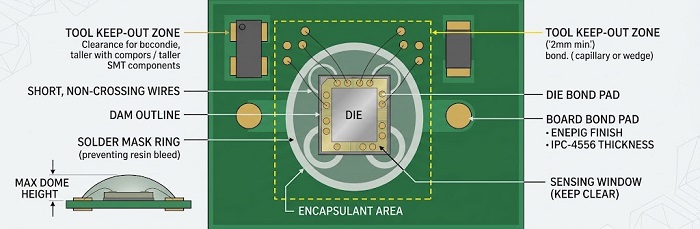
Solder first, bond second. Complete SMT reflow and cleaning before die attach and wire bonding, so flux residue never reaches the bond pads.
Specify a bondable finish. Use ENEPIG or soft gold for gold ball bonding, and call out deposit thicknesses per IPC-4556 rather than nominal values.
Leave tool clearance. Keep tall SMT parts out of a keep-out zone around the die, sized to the capillary or wedge tool being used.
Size the bond pads. Make board pads larger than the die pads, keep wires short, and avoid wire crossings.
Define the encapsulant boundary. Show the dam outline and maximum dome height on the assembly drawing, and use a solder mask ring to stop resin bleed.
Protect sensing areas. Mark any region that must remain unencapsulated and specify a lid or window approach.
Control flatness. Plan for panel warpage during cure; synthetic stone fixtures hold boards flat through thermal steps.
Plan for flexible substrates. If the module uses a flex or rigid-flex substrate, keep the die off active bend zones or add local stiffening.
Confirm die supply. Specify known-good die (KGD) or wafer-sort testing, plus storage and moisture-handling requirements.

Submit Your COB Project for Engineering Review
The right COB approach depends on your die, substrate finish, encapsulant, and the reliability profile of your target industry. Send your Gerber files, BOM, assembly drawing (including the bond diagram and encapsulant outline), and environmental requirements. Our engineering team will review DFM and confirm which steps of your COB flow fall within our assembly scope.
Helpful Resources
Advanced PCB Assembly Capabilities
Printed Circuit Board Assembly Inspection Methods
Quality Documentation & Traceability Requirements for Semiconductor Test Equipment OEMs


