



First pass yield (FPY) improvement in PCBA is one of the few quality metrics that translates directly into program economics: every board that fails first-pass inspection or test consumes rework labor, re-inspection cycles, and — in diagnostic instrument programs where traceability and functional verification are non-negotiable — additional documentation overhead. For engineering teams supporting life sciences and diagnostic instrument electronics, treating FPY improvement as an ad hoc "fix the loudest defect" exercise tends to produce short-lived gains. A structured FPY framework for medical electronics produces improvements that hold across product revisions and volume changes.
This article outlines a defect root cause framework for categorizing FPY-influencing factors, prioritizing improvement opportunities, and using inspection data to localize where in the process defects actually originate — a methodology any diagnostic instrument PCBA program can apply regardless of EMS provider.
Why First Pass Yield Deserves Structured Analysis
In high-mix, low-volume (HMLV) PCBA programs, FPY problems rarely have a single root cause. A diagnostic instrument board might combine fine-pitch QFN packages, mixed SMT/THT construction, and conformal coating steps — each contributing its own defect population. Without a categorization framework, engineering teams tend to chase the most visible defect type rather than the one with the greatest cost impact, and improvement actions get applied inconsistently across product families.
A structured framework does three things: it separates symptoms (solder bridging, insufficient wetting, tombstoning) from underlying causes (design, process, material, inspection gap); it creates a repeatable prioritization logic instead of relying on engineering intuition alone; and it produces an audit trail that supports design-for-manufacturability (DFM) feedback loops with the OEM's design team.
A Four-Category Framework for FPY-Influencing Factors
Most FPY detractors in diagnostic instrument PCBA fall into four categories. Treating them separately keeps root cause analysis from collapsing into a single generic "process issue" bucket.
Design Factors (DFM)
Design-stage decisions frequently determine whether a defect is even correctable through process adjustment. Common design-driven FPY detractors include:
Insufficient thermal relief or copper balance leading to warpage during reflow
Component footprint deviations from manufacturer land pattern recommendations
Inadequate spacing for fine-pitch components relative to stencil aperture tolerances
Test point placement that limits ICT or flying probe coverage
Because these issues originate before the board reaches the assembly floor, they are best addressed through a formal DFM review cycle rather than production-floor workarounds.
Process Factors
Process-driven defects are the category most directly controllable by the EMS provider. Relevant variables include:
Reflow profile parameters (ramp rate, soak time, peak temperature) relative to paste manufacturer specifications — deviation is a common contributor to insufficient wetting and voiding
Stencil design (aperture ratio, thickness) relative to paste deposition accuracy, particularly for fine-pitch passives and QFN thermal pads
Selective wave soldering parameters for mixed-technology boards, including nitrogen atmosphere control to reduce bridging and dross formation
Fixture-related warpage during reflow on large or asymmetric board designs
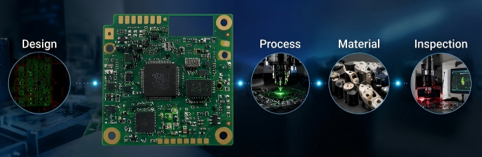
Incoming Material Factors
Component and substrate quality entering the line contributes to FPY in ways that are easy to underweight during root cause analysis:
Moisture-sensitive device (MSD) handling deviations leading to popcorning during reflow
Solder paste shelf-life or storage condition deviations affecting print consistency
PCB surface finish variability affecting solderability
Component coplanarity issues on BGA/QFN packages, which are frequently invisible until X-ray inspection
Inspection Coverage Factors
The final category is not a defect source itself but a detection gap: FPY figures are only as meaningful as the inspection strategy behind them. A board with a real defect population but limited inspection coverage will show a misleadingly favorable FPY number, while defects surface later in functional test or field use.
Programs that are seeing recurring FPY issues across one or more of these four categories often benefit from a structured review before committing to a redesign or process change — reach out to PCBCart's engineering team to discuss your specific defect profile.
Prioritizing Improvement Opportunities: Frequency × Repair Cost
Once defects are categorized, the next step is prioritization. Not every defect category deserves equal engineering attention — a low-frequency defect with high repair cost may warrant faster action than a high-frequency, low-cost defect that is already contained by existing rework procedures.
A practical prioritization matrix ranks improvement opportunities along two axes:
Defect frequency — how often a given defect type appears across a representative sample of builds for a given product family
Repair cost — the combined cost of rework labor, component replacement, re-inspection, and any re-test or re-documentation required for regulated products

Plotting defect categories against these two axes produces four general zones for action:
High frequency, high repair cost — top priority; typically warrants a DFM or process change rather than continued rework
High frequency, low repair cost — worth addressing for throughput, but rarely urgent from a cost standpoint
Low frequency, high repair cost — worth root-causing individually, since a single occurrence can be expensive even if rare (BGA rework on a densely populated board is a representative example)
Low frequency, low repair cost — generally monitored rather than actively engineered against
This matrix should be rebuilt periodically, since defect populations shift as product designs mature and component sourcing changes.
Using Inspection Data to Localize Defect Origin
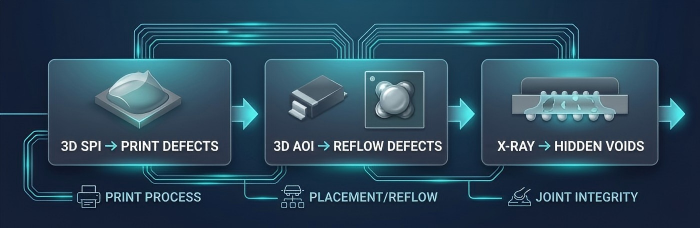
Determining where in the process a defect originates is a separate question from identifying that a defect exists. A structured inspection sequence — 3D Solder Paste Inspection (SPI) immediately after print, 3D Automated Optical Inspection (AOI) post-reflow, and off-line X-ray for BGA/QFN voiding and hidden joint conditions — creates a data trail that can be used methodologically, without requiring proprietary statistics, to narrow down process stage:
SPI-flagged deviations (paste volume, height, or offset outside tolerance) point toward stencil design, print parameters, or paste condition rather than reflow or component issues
AOI findings that were not flagged at SPI suggest the defect originated during reflow or placement rather than at print
X-ray findings on joints that passed AOI — such as BGA voiding or head-in-pillow conditions — indicate a defect category that is inherently invisible to optical inspection and requires oblique-angle X-ray to characterize accurately
Cross-referencing defect location against UID-level traceability in the MES allows engineering to determine whether a defect pattern correlates with a specific reel, feeder position, or production shift, rather than being distributed randomly across the build
This closed-loop approach — SPI, AOI, and X-ray data reviewed together rather than in isolation — is what allows a defect to be attributed to a process stage with reasonable confidence, without relying on speculative root cause assignment.
Diagnostic instrument PCBA programs carry tighter tolerance for undetected defects than general industrial electronics, given downstream functional test and regulatory documentation requirements. If recurring defects are eating into your program's margin through rework and re-test cycles, a structured FPY review is often the fastest way to identify where the highest-value fix sits.
Ready to apply this framework to your program? Request an FPY improvement evaluation with PCBCart's engineering team.
Helpful Resources
● Navigating ISO 13485 Principles with an IATF 16949 Certified PCBA Partner
● Comparison of AOI, ICT and AXI and When to Use Them during PCB SMT Assembly
● Mitigating Moisture Sensitivity Level (MSL) Risks in High-Density SMT Assembly


