



Conformal coating is standard practice for industrial IoT PCBA deployed in humid, dusty, or chemically exposed field environments — but boards carrying an antenna, RF connector, or high-frequency matching network need a design control that general-purpose coating specs don't address: a defined keep-out zone. Without one, the coating process and the RF design can work against each other, and the result is a board that passes visual coating inspection but underperforms on signal.

Why Conformal Coating and RF Regions Conflict
Conformal coatings — acrylic, silicone, urethane, or parylene — are applied to industrial IoT PCBA to protect against humidity, dust, and chemical exposure in field-deployed enclosures (gateways, sensor nodes, remote I/O modules). Every one of these materials has a dielectric constant well above that of air, typically in the 3–4 range depending on chemistry and cure state.
An antenna — whether a printed PCB trace antenna, a chip antenna, or the immediate ground clearance and matching network feeding an external antenna connector — is tuned assuming a specific surrounding dielectric environment, usually air plus the PCB substrate. Introducing a uniform coating layer over that geometry changes the effective permittivity the radiating element sees. The practical consequences, described qualitatively rather than with invented figures, are:
Resonant frequency shift. A dielectric loading effect pulls the antenna's resonant point downward from its designed center frequency, which can push it outside the intended ISM or cellular band edge.
Increased return loss / higher VSWR. As the antenna moves off-tune, more of the transmitted energy reflects back into the front-end rather than radiating, degrading both transmit efficiency and receiver sensitivity.
Reduced radiation efficiency. Lossy coating chemistries (particularly those with higher tan δ at RF frequencies) absorb a portion of the field rather than letting it radiate, which is distinct from and additive to the detuning effect above.
Non-uniform coating thickness compounding the problem. Because coating thickness is rarely perfectly uniform across a board, the detuning effect is not a fixed, predictable offset — it varies board to board unless the coating boundary and thickness are both controlled at the region in question.
None of these effects are unique to any one coating chemistry; the direction of the effect (lower resonant frequency, higher loss) is well documented in RF design literature. The magnitude for a specific antenna geometry depends on coating thickness, dielectric constant, and how close the coating approaches the radiating element and its ground clearance — which is exactly why a defined keep-out boundary, rather than a "coat everything except the connector" instruction, is the correct design control.
Defining the Keep-Out Boundary
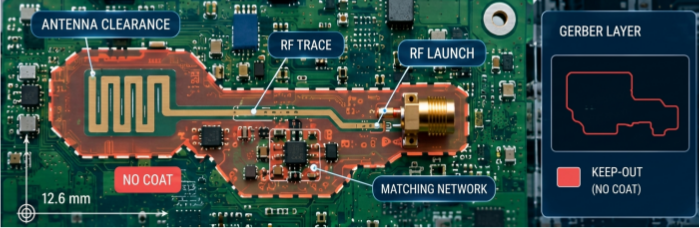
Keep-out zones for RF regions are not a single ring around the antenna footprint — they are a set of related exclusion areas that should each be called out explicitly on the fab/assembly drawing and, ideally, as a distinct Gerber layer.
Antenna Near-Field Clearance
For a printed PCB antenna (PIFA, monopole, meandered trace), the keep-out region typically extends beyond the visible copper of the antenna element itself to include the antenna's ground clearance area underneath and adjacent to it — the area intentionally left free of ground plane to allow the antenna to radiate. Coating that bridges this clearance changes its effective dielectric loading even where no copper is present.
RF Connector and Launch Region
Where an external antenna connects via a U.FL, SMA, or MHF connector, the keep-out zone should extend from the connector footprint back along the RF trace to the point where the trace transitions from a controlled-impedance microstrip/coplanar waveguide to a general-purpose signal trace. Coating over a controlled-impedance line changes its effective dielectric constant and therefore its characteristic impedance, degrading the match between the transmission line and the connector/antenna.
High-Frequency Trace Runs
Any trace carrying signals at the operating RF frequency (not just the final antenna feed) — including matching network component pads (pi/L-network capacitors and inductors) — should be included in the exclusion zone. Coating over discrete matching components changes their effective parasitic capacitance to ground, shifting the match point the network was tuned to achieve.
Documentation Practice
Mark the keep-out boundary as a dedicated mechanical/documentation layer in the Gerber set (e.g., a "No Coat" or "Keep-Out — Conformal Coating" layer), distinct from the solder mask and assembly outline layers.
Reference the boundary explicitly in the assembly drawing notes, with a callout dimension from a fiducial or component reference rather than a vague "avoid antenna area" instruction.
Where the keep-out region is irregular (following a meandered trace antenna), provide the boundary as a closed polygon rather than a simple bounding box, so the exclusion is no larger than necessary — an oversized keep-out area creates unnecessary unprotected copper elsewhere on the board.
Selective Coating Process Execution
Boundary-accurate execution is a process capability question as much as a design question. Two coating approaches are commonly used in HMLV PCBA production, with different implications for RF keep-out accuracy:
Spray coating with masking. A physical mask (tape, silicone boot, or custom fixture) is placed over the keep-out region before spraying, then removed after cure. This works but adds a masking/demasking step per board, introduces mask-alignment variability, and risks adhesive residue or coating creep under the mask edge on fine-pitch RF layouts.

Selective jet dispensing. A programmable jet dispensing platform — the same class of equipment (MYCRONIC jet printer/dispenser platform) used for selective solder paste and adhesive dispensing in SMT — can be programmed with the keep-out polygon directly from the design data, dispensing coating material only within the defined coating area and stopping precisely at the boundary. Jet-based selective dispensing platforms of this type are typically specified with droplet placement accuracy on the order of ±0.1mm, which is materially tighter than a physical mask edge can reliably hold, particularly around a meandered antenna trace with narrow re-entrant clearance regions.
The practical advantage of jet dispensing for RF keep-out work is that the boundary is defined in software from the same coordinate data as the Gerber keep-out layer, removing the mask-alignment step as a source of boundary variation — rather than relying on a fixture that has to be re-registered to the board on every cycle.
Post-Coating Verification
Most conformal coating materials used in electronics assembly include a UV-fluorescent tracer additive, allowing coverage to be inspected under UV illumination after cure — this is standard industry practice per IPC-CC-830 guidance on coating inspection, not a proprietary test method. For RF-adjacent boards, this inspection step serves two purposes simultaneously:
Coverage confirmation — verifying the coated area meets the required protection boundary and film thickness expectations, with no voids, bubbles, or thin spots in the protected region.
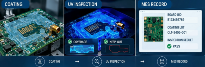
Keep-out confirmation — verifying, under the same UV inspection, that no coating fluorescence is visible inside the defined keep-out polygon around the antenna, RF connector, and high-frequency trace regions.
This is a manufacturing-record inspection step performed against the board's own design documentation — it confirms that the coating process executed to the defined boundary, not that the resulting board meets a specific RF performance specification or EMC compliance limit. RF performance verification (return loss, radiated efficiency) remains the customer's or a certified test lab's responsibility; PCBCart's inspection process is a production-line coverage/keep-out check, not an accredited RF or EMC measurement.
Inspection results and coating lot/material batch information are logged in the assembly's MES record alongside the board's UID, so a specific unit's coating process history is traceable if a field issue is later reported.
RF Board Coating Design Checklist
Before releasing a coating spec for an RF-containing industrial IoT board, confirm:
Antenna near-field clearance is included in the keep-out polygon, not just the visible antenna copper.
RF connector launch region and controlled-impedance trace run back to the impedance transition point are excluded.
Matching network component pads are excluded, not just the antenna feed trace.
The keep-out boundary is provided as a dedicated Gerber/documentation layer with a closed polygon, not a text note.
The coating method selected (selective jet dispensing vs. masked spray) matches the geometric complexity of the keep-out boundary.
Post-cure UV inspection criteria explicitly include a keep-out check, not coverage confirmation alone.
A keep-out design flaw on an RF board is expensive to catch late — antenna detuning or lot-to-lot coating thickness drift is far cheaper to prevent at the design stage than to rework after coating. If your industrial IoT board includes an antenna, RF connector, or high-frequency matching network, it's worth reviewing the coating approach before your project goes into production — confirming the keep-out boundary is properly documented and that the selective coating method matches your board's geometry. Submit your project for a coating process evaluation →
Helpful Resources
• Guidelines for RF and Microwave PCB Design
• Thermal Cycling Reliability for Outdoor Power Electronics Enclosures: Conformal Coating & Potting Strategy
• PCBA Conformal Coating for Industrial Automation Reliability
• General Aspects You Should Know about Conformal Coating Applied on PCB
• First Article Inspection Service on all PCB Assembly Orders
• Free DFM Check


